

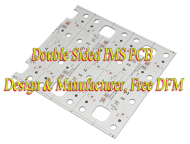
How to design double sided IMS PCB? This blog is mainly about its stackup, spec, difference between FR4 PCB, design guide.
Are you troubled with these questions?
- Why are your double-sided IMS PCB manufacturing costs spiraling out of control? Are layer alignment and via plating complexity threatening your project budget?
- Is uneven heat distribution causing decreased product reliability? Is improper dielectric layer selection exacerbating heat dissipation problems?
- Are via failures in harsh environments causing a surge in customer complaints? Are vibration and corrosion threatening product lifespan?
As a professional IMS PCB manufacturer, EBest Circuit (Best Technology) can provide you solutions:
- Cost Reduction: Replace copper-based substrates with aluminum substrates (cost reduction of 30%+), and work with suppliers to optimize non-critical design elements (such as reducing redundant plating layers and simplifying layer structures), directly reducing process complexity and material costs.
- Heat Dissipation Optimization: Use polyimide dielectric layers with a thermal conductivity ≥3W/mK, ensuring uniform width and thickness of copper traces on both sides to guarantee a uniform heat diffusion path and avoid localized hot spots.
- Through-Hole Reinforcement: Clearly require a “plated through-hole + solder mask coverage” process. The solder mask provides physical/chemical protection, and the plated through-hole enhances mechanical strength, providing double protection against vibration and corrosion, extending product lifespan.
Welcome to contact us if you have any request for IMS circuit board: sales@bestpcbs.com.
What Are Double Sided IMS PCBs?
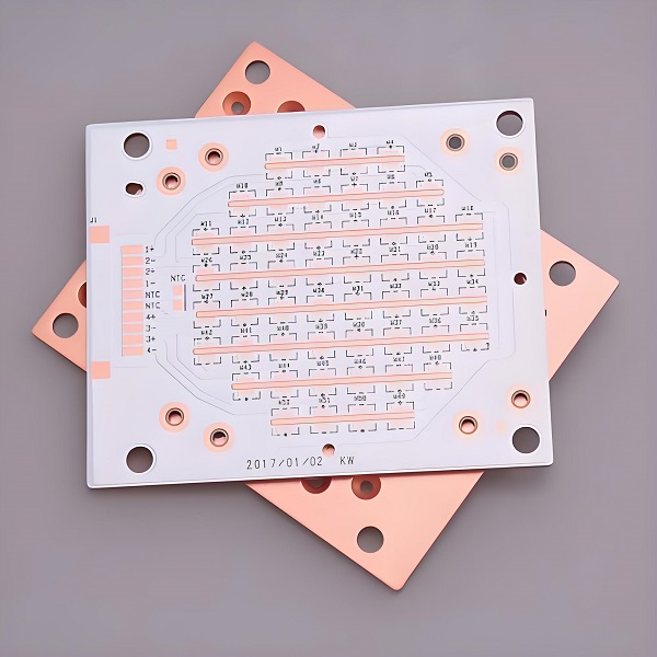
Double sided IMS PCB (Metal Insulated Substrate Printed Circuit Board) is a special type of circuit board that uses a metal (such as aluminum) as the substrate and features double-sided wiring. Interconnection between the two sides is achieved through metallized vias, offering both high heat dissipation performance and wiring flexibility.
Its core advantages includes the metal substrate (such as aluminum) provides excellent heat dissipation, making it suitable for high-power radio frequency (RF) devices; the double-sided wiring design significantly increases circuit density, supporting complex high-frequency signal transmission; and via technology ensures reliable interlayer electrical connections. Typical applications include LED lighting, motor drives, and RF power modules.
Double-Sided IMS PCB Stackup
1. Top Solder Mask
- Material: Photosensitive ink.
- Thickness: 20-25μm.
- Function: Protect copper traces and define pad areas.
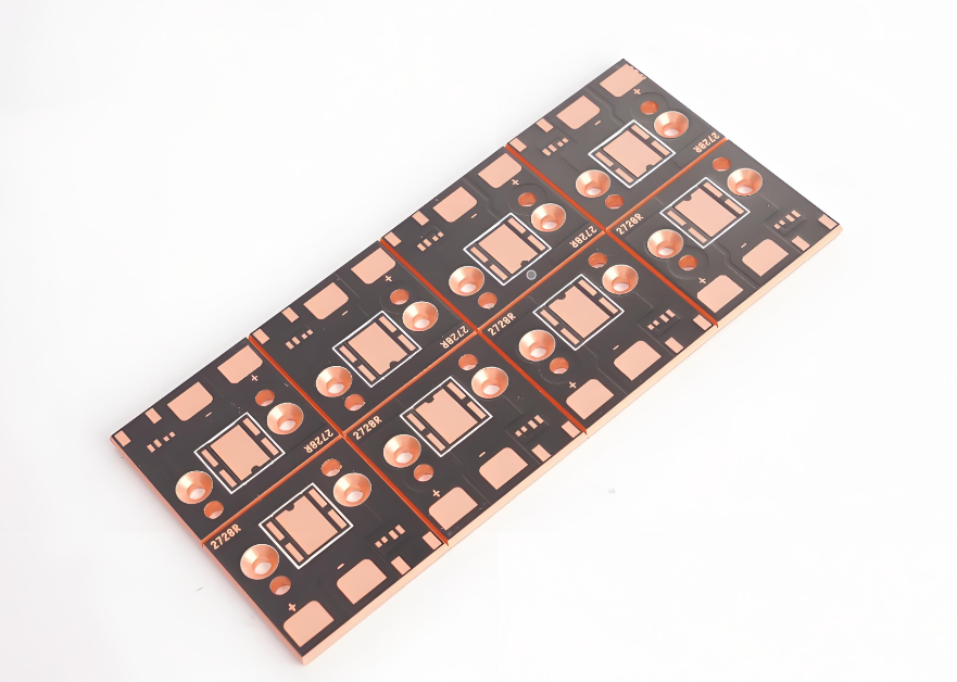
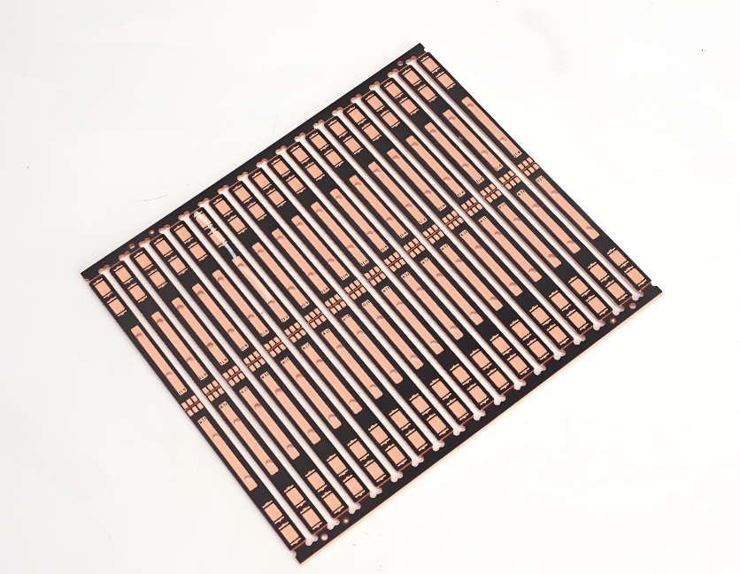
2. Top Copper Layer
- Copper thickness: 1oz/2oz (35/70μm customizable)
- Characteristics: Accommodates LEDs, ICs and other heat-generating components, supports high-precision etching (minimum line width/spacing 0.1mm).
3. Thermal Dielectric Layer
- Material: Modified epoxy resin with ceramic fillers.
- Thickness: 75-150μm (±10%).
- Parameters: Thermal conductivity ≥ 2.5 W/(m·K), breakdown voltage > 3kV.
4. Metal Core
- Material: Aluminum alloy 6061T6 (or optional copper base).
- Thickness: 1.0-3.0mm (1.6mm recommended for keyboards).
- Function: Primary heat dissipation channel and structural support.
5. Bottom Dielectric
- Material/Thickness: Same as top dielectric layer (symmetric structure ensures thermal balance).
6. Bottom Copper Layer
- Copper thickness: 1oz/2oz.
- Function: Accommodates MCUs, connectors and other components, connects to top layer via thermal PTHs.
7. Bottom Solder Mask
- Thickness: 20-25μm.
- Additional feature: Partial windowing for enhanced heat dissipation (copper exposure ratio < 30%).
Double Sided IMS PCB Specifications
| Parameter | Specification / Range |
| Metal Substrate Type | Aluminum or Copper Alloy |
| Metal Substrate Thickness | 0.8 mm – 3.0 mm (standard), up to 6.0 mm (custom) |
| Dielectric Layer | Polymer-ceramic composite |
| Dielectric Thickness | 0.075 mm – 0.15 mm |
| Thermal Conductivity (k) | 0.8 – 3.0+ W/mK (standard), >5 W/mK (high-performance) |
| Copper Foil Thickness | 1 oz (35 μm), 2 oz (70 μm), 3 oz (105 μm); 0.5–4 oz+ custom |
| Breakdown Voltage (BDV) | >1.5 kV, >2 kV, >3 kV, >4 kV (standard grades) |
| Dielectric Constant (Dk) | 3.0 – 5.0 (@1MHz) |
| Dissipation Factor (Df) | 0.02 – 0.05 (@1MHz) |
| CTI Rating | >600 V (high-reliability), >400 V, >250 V |
| CTE (Z-axis) | Higher than standard FR-4 (material-dependent) |
| Tg (Dielectric) | >130°C, >150°C |
| Finished Board Thickness | 1.0 mm – 4.0 mm (typical) |
| Max Panel Size | 457 × 610 mm (18″ × 24″), 533 × 610 mm (21″ × 24″) |
| Min. Trace/Space | 6/6 mil (0.15/0.15 mm) standard; 4/4 mil (0.10/0.10 mm) advanced |
| Min. Drill Size | 0.3 mm (mechanical), 0.2 mm (advanced) |
| Surface Finishes | ENIG, OSP, Immersion Ag/Sn, Exposed Pad (thermal pads) |
| Solder Mask | LPI (all colors), min. dam: 0.1 mm |
| Silkscreen | Epoxy ink, min. line/height: 0.15 mm |
| Thermal Via Recommendation | Required under high-power components (filled/plugged) |
| Insulation Moat | Optional for electrical isolation |
| Certifications | UL 94V-0, IPC-4101, ISO 9001, IATF 16949 (automotive) |
| Thickness Tolerance | ±10% (standard), ±0.1 mm (precision) |
| Outline Tolerance | ±0.15 mm (standard), ±0.10 mm (precision) |
Double Sided IMS PCB vs. FR4 PCB: Which Is Better?
A Detailed Selection Guide Between Double Sided IMS PCB and FR4 PCB:
1. Thermal Management Capability
- Double-Sided IMS PCB: Metal substrate (aluminum/copper) combined with high thermal conductivity dielectric layer achieves thermal conductivity of 1–7 W/m·K, rapidly dissipating heat across the substrate. Ideal for high-power density devices (LEDs, power modules, automotive electronics) to reduce operating temperatures.
- Traditional Double-Sided FR-4 PCB: FR-4 substrate offers only ~0.25 W/m·K thermal conductivity. Heat relies on copper traces and thermal vias, prone to localized hotspots in high-power scenarios, requiring external heatsinks or forced air cooling.
2. Mechanical Strength and Durability
- IMS PCB: Metal substrate delivers superior rigidity, vibration resistance, and shock tolerance, suitable for harsh environments (automotive, industrial equipment) with long-term reliability.
- FR-4 PCB: Glass-fiber epoxy substrate experiences reduced mechanical strength in thin profiles. High reliability demands thicker layers or stiffeners, increasing weight and cost.
3. Circuit Density and Design Flexibility
- Double-Sided IMS PCB: Supports dual-sided SMD placement for high component density. Limited to single/double-sided dielectric layers, restricting multi-layer signal expansion compared to FR-4.
- Traditional Double-Sided FR-4 PCB: Utilizes plated through-holes (PTH) for inter-layer connectivity, enabling scalable 4-layer/6-layer+ designs with greater routing freedom for complex digital/high-frequency/mixed-signal circuits.
4. High-Frequency and Signal Integrity
- IMS PCB: Metal substrate introduces significant parasitic capacitance, causing signal loss and impedance fluctuations above 1 GHz. Requires specialized ground plane and shielding designs.
- FR-4 PCB: Stable dielectric constant facilitates impedance control and low-loss transmission, widely adopted in RF, microwave, and other high-frequency applications.
5. Cost Structure
- IMS PCB: High material costs (metal substrate, specialty dielectrics) and complex processing (metal machining, laminate bonding) result in 20–50% higher per-unit costs versus equivalent FR-4.
- FR-4 PCB: Mature raw materials (glass cloth + epoxy) and extensive supply chains drive significant cost advantages for volume production, ideal for budget-sensitive projects.
6. Manufacturing and Assembly Considerations
- IMS PCB: Primarily supports SMD assembly due to metal substrate limitations for PTH. Through-hole components require localized FR-4 sub-panels, adding process steps.
- FR-4 PCB: Mature PTH technology supports mixed SMD/through-hole assembly with straightforward, universal processes.
7. Typical Application Scenarios
- Prefer Double-Sided IMS PCB: High-power LED lighting, automotive power controllers, industrial inverters, power semiconductor heat spreaders, and any scenario demanding high thermal conductivity/mechanical robustness.
- Prefer Traditional Double-Sided FR-4 PCB: Consumer electronics (smartphones/motherboards), communication devices, RF modules, multi-layer laminates, complex signal conditioning, and cost-sensitive applications with manageable thermal loads.
8. Selection Recommendations
- High power density, thermal bottlenecks, vibration/shock environments: Prioritize double-sided IMS PCB for active thermal management and enhanced reliability.
- Complex signaling, multi-layer routing, budget constraints, conventional thermal loads: Opt for traditional double-sided FR-4 PCB for economic flexibility.
- Hybrid high thermal conductivity + multi-signal layer requirements: Consider IMS-FR-4 hybrid panel designs, though this increases process complexity and costs.
Double Sided IMS PCB Design Guidelines
Below Is A Guide for Doubled Sided IMS PCB Board:
1. Design Fundamentals and Material Selection
- Substrate Material: High-thermal-conductivity metal substrates (aluminum/copper) with thicknesses of 0.8–3.5mm, complying with IPC-4101 standards. Insulation layers use ceramic-filled polymers (e.g., boron nitride/alumina) with thermal conductivity of 1.0–10W/mK, 3–10 times higher than FR4.
- Copper Foil Process: Top/bottom layer copper thicknesses of 1–2oz (0.035–0.07mm). Critical power device areas adopt 2oz copper to reduce impedance. Surface treatments recommend immersion gold/silver for high-temperature resistance and RoHS compliance.
2. Layer Structure and Thermal Management
- Layer Layout: High-speed signal traces on the top layer, power/ground planes on the bottom layer. Metal substrates act as heat dissipation layers, isolated from circuit layers by thermal insulation. Thermal via arrays (φ0.3–0.5mm, pitch 1.5mm) connect layers, reducing thermal resistance by 50%.
- Heat Dissipation Optimization: Power devices use grid copper areas (2oz thickness) paired with aluminum heatsinks (thermal resistance <1℃/W). High-heat zones employ embedded copper blocks (1–3mm thickness) with vent holes to prevent solder defects.
- Thermal Simulation: ANSYS Icepak verifies steady-state thermal distribution, ensuring 15W-class device hotspots stay below 85°C. Transient thermal shock tests meet MIL-STD-883G standards (−55°C to 125°C cycling for 500 cycles without cracks).
3. Electrical Performance and Routing Rules
- Signal Integrity: High-speed signal line widths ≥0.2mm, differential pair impedance controlled at 100±10Ω. Critical signals follow 3W routing principles, avoiding 90° corners; use 45° miters or arcs instead.
- Power Design: Power planes are segmented clearly, with ≥2mm-wide copper for high-current paths. Ground planes maintain integrity, with via arrays enabling low-impedance return paths.
- EMI Control: High-frequency components (e.g., crystals) use external filter capacitors and are placed away from analog circuits. Sensitive signal lines flank GND via arrays (spacing ≤200mil) to suppress crosstalk.
4. Manufacturing Process and Testability
- Drilling Process: Mechanical holes range from 0.3–0.8mm diameter, with copper plating thickness ≥20μm. Laser microvias suit high-density designs, with impedance fluctuations within ±5%.
- Surface Finishes: Immersion gold layers are 1–3μm thick, with nickel layers of 10–15μm, passing 96-hour salt spray tests. OSP suits short-term storage (≤3 months) with lower costs.
- Testing Standards: Continuity tests verify via resistance <50mΩ and insulation resistance >1GΩ. AOI checks line width deviations ≤±10%, while thermal imaging validates uniform heat dissipation.
5. International Standards and Best Practices
- Compliance: Adheres to IPC-4101 substrate specifications, UL 796 insulation certifications, and EU CE directives. Automotive electronics pass AEC-Q200 durability tests.
- Design Verification: Altium Designer performs 3D thermal-electrical co-simulation. Gerber outputs include solder mask, silkscreen, and drill files. Panelization uses V-CUT or stamp holes, with edge-to-component spacing ≥2mm.
- Case Studies: LED driver modules use 1.0mm aluminum substrates + 0.15mm insulation, reducing thermal resistance by 90% versus FR4. Power modules maintain temperatures below 65°C via thermal via arrays, improving efficiency by 20%.
Case Studies of Our Double Sided IMS PCB Board
Project Background
- The client is a European industrial automation equipment manufacturer that needs to develop a main control board for its next-generation high-temperature motor driver.
- This driver needs to operate continuously at ambient temperatures up to 85°C, and the power module generates over 25W of heat. Traditional FR-4 board material, due to its low thermal conductivity (approximately 0.3W/m·K), is insufficient to meet the heat dissipation requirements.
- The client requires the PCB to achieve double-sided mounting within a limited space (120mm × 80mm) to accommodate more signal conditioning and protection circuitry.
Project Challenges
- High Heat Flux Density Heat Dissipation – The power MOSFETs and driver ICs are concentrated in a localized area, where temperatures may exceed 125°C. Single-sided heat dissipation on a standard aluminum substrate is insufficient.
- Double-Sided Interconnect Reliability – Double-sided IMS requires metallized vias to connect the traces on both sides. However, the significant difference in the coefficient of thermal expansion (CTE) between the aluminum substrate and copper foil can easily lead to via wall breakage after repeated reflow soldering.
- Signal Integrity – High-frequency switching noise (-200kHz) generated by the motor drive can easily interfere with adjacent sensitive analog signal lines.
- Cost and Delivery Time Pressures – The customer requires samples to be completed and ready for mass production within 6 weeks.
Solutions
- Board Selection – Double-sided aluminum-based IMS is used, with a thermal conductivity of 2.0 W/m·K, a dielectric layer thickness of 100µm, and copper thickness of 1oz/35µm, ensuring effective heat conduction on both upper and lower layers.
- Visor Structure Optimization – Copper-filled blind vias (laser drilling) are used to connect upper and lower layers, avoiding cracking of through-holes due to CTE mismatch; the copper plating thickness on the via walls is >25µm, improving mechanical strength.
- Layer Stack-up and Shielding Design – A “signal-ground-signal” layer stack-up (6 layers in total) is adopted, with a ground plane on the inner layer. Critical analog traces are grounded and additional copper shielding is added to reduce crosstalk.
- Collaborative Design and Rapid Prototyping – Early collaboration with the PCB manufacturer, adjusting trace width/spacing to ≥4mil through DFM analysis to avoid production risks; rapid prototyping service (10-day delivery) is used to verify the design.
Results and Outcomes:
- Heat Dissipation Performance – Under full load, the junction temperature of power devices is controlled below 98°C, a reduction of 32°C compared to the original FR-4 design.
- Reliability Improvement – No microcracks were observed in vias after 1000 temperature cycling cycles (-40°C to +125°C).
- Signal Quality – Switching noise coupling voltage on analog signal lines is <5mV, meeting customer EMC Class B requirements.
- Project Cycle – From design to sample verification, it took only 5 weeks, and subsequent mass production yield remained above 99.2%.
Why Choose EBest Circuit (Best Technology) as IMS PCB Manufacturer?
Reasons Why Choose EBest Circuit (Best Technology) as IMS PCB Manufacturer:
- 19 Years of Expertise in Double-Sided IMS PCB: Specialized in metal-core PCB for 19 years, with over 5,000 high-power density project cases, ensuring complex designs are manufactured flawlessly.
- Free DFM Analysis for Design Optimization: Professional engineers provide free Design for Manufacturability analysis to identify risks like line width/spacing issues and thermal stress points, reducing trial costs by over 30%.
- 24-Hour Rapid Prototyping Delivery: From design files to sample boards in 24 hours, meeting urgent validation needs for high-power modules and automotive electronics to accelerate time-to-market.
- 24/7 Expert Team Support: Senior engineers offer real-time technical support covering material selection (aluminum/copper base), via size optimization, and thermal path design to ensure precise implementation of design intent.
- Transparent Pricing with No Hidden Fees: Quotes include all process costs (via plating, lamination, solder mask windowing) with no additional charges, priced 15%-20% lower than comparable double-sided IMS products for predictable budgeting.
- Rigorous Quality Control System: ISO 9001/14001 certified, with dual checks via inline AOI inspection and final electrical testing to guarantee stable thermal conductivity ≥2.5W/(m·K) and breakdown voltage >3kV.
- Superior Thermal Management with Double-Sided Structure: Metal core thickness 1.0-3.0mm (1.6mm recommended for keyboards) combined with thermal via arrays reduces thermal resistance by 40%, ideal for 5G modules and GaN power devices.
- Material and Process Compatibility Verified: Supports customizable copper thickness (1oz/2oz), lead-free soldering, and compliance with RoHS/REACH standards for medical, automotive, and industrial control applications.
- Full-Cycle Responsive Support: From prototyping to mass production, including small-batch trials, process fine-tuning, and reliability testing (thermal shock, salt spray) to ensure manufacturing stability.
- Proven Success and Long-Term Partnerships: Serving top 10 global PCB design firms with over 85% repeat purchase rate, providing end-to-end services from design to production to reduce supply chain management costs.
Our IMS PCB Board Manufacturing Capabilities
| Base material | Copper |
| Thermal Conductivity (dielectric layer): | 0.8, 1.0, 1.5, 2.0, 3.0 W/m.K. |
| Board Thickness: | 0.5mm~3.0mm(0.02″~0.12″) |
| Copper thickness: | 0.5 OZ, 1.0 OZ, 2.0 OZ, 3.0 OZ, up to 10 OZ |
| Outline: | Routing, punching, V-Cut |
| Soldermask: | White/Black/Blue/Green/Red Oil |
| Legend/Silkscreen Color: | Black/White |
| Surface finishing: | Immersion Gold, HASL, OSP |
| Max Panel size: | 600*500mm (23.62″*19.68″) |
| Packing: | Vacuum/Plastic bag |
| Samples L/T: | 4~6 Days |
| MP L/T: | 5~7 Days |
How to Get a Quote for IMS PCB Project?
All Material Required for IMS PCB Project:
- Project Specification Document: Define the number of layers, dimensions, thickness, material type (e.g., aluminum-based, copper-based), insulation layer thickness, and performance requirements for the IMS PCB.
- Design Files: Provide complete Gerber files, Excellon drill files, stack-up diagrams, and solder mask design drawings.
- Bill of Materials (BOM): List all electronic components with models, specifications, quantities, and special requirements (e.g., high-temperature resistance, high thermal conductivity).
- Surface Treatment Requirements: Specify coating types (e.g., HASL, ENIG, OSP), solder mask color, marking specifications, and solderability test standards.
- Electrical Performance Parameters: Include impedance control requirements, signal integrity analysis, thermal management needs (e.g., thermal conductivity, heat dissipation design), and power capacity.
- Certification and Compliance Documents: Provide international certifications (e.g., RoHS, REACH, UL) and compliance declarations for target market regulations.
- Sample or Prototype Requirements: If sample validation is needed, specify the quantity, testing items, and acceptance criteria.
- Packaging and Shipping Requirements: Clarify packaging methods (e.g., anti-static, moisture-proof), shipping methods (air/sea freight), insurance, and tariff responsibilities.
- Quality Assurance Agreement: Include quality inspection standards (e.g., IPC standards), defect rate control, repair policies, and warranty periods.
- Commercial Terms: Define the quote validity period, payment methods (e.g., T/T, L/C), lead time, minimum order quantity, and price terms (EXW/FOB/CIF).
Welcome to contact us if you have any request for IMS printed circuit board: sales@bestpcbs.com.