

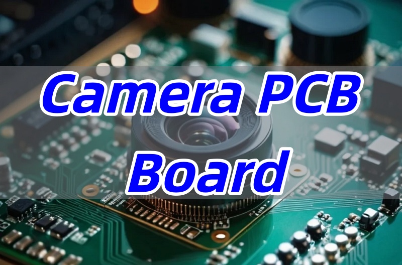
A camera PCB board (Printed Circuit Board) is the central nervous system of any imaging device, responsible for interconnecting components like image sensors, processors, and connectors to capture and process visual data. This article provides a comprehensive guide, walking through the entire journey of a camera PCB board from its initial prototype phase to a fully assembled and functional unit, covering key aspects like design, functionality, and cost.
Are you struggling to bridge the gap between a camera PCB design and a reliable, mass-produced camera PCB board?
- Unclear Design Specifications: Vague requirements for different camera types (e.g., CCTV camera PCB board, WiFi camera circuit board) lead to incompatible components and performance issues.
- Signal Integrity Problems: Inadequate camera PCB design for high-speed data transmission results in noisy images, dropped signals, and poor video quality.
- Component Sourcing Difficulties: Finding reliable suppliers for critical parts like the camera sensor PCB, especially for specific voltages like a 12v camera PCB board or a 3.3v camera PCB board, can be time-consuming and risky.
- Cost Overruns: Unexpected complexities in prototyping and scaling up manufacturing can make the final camera PCB board price exceed projections significantly.
- Manufacturing and Assembly Defects: Issues like improper soldering or layer misalignment during production lead to high failure rates, whether you need a new camera PCB board or a replacement camera PCB board.
Addressing these challenges requires a partner with robust engineering and manufacturing capabilities. Here are five key solutions that a professional PCB manufacturer provides.
- Requirement Analysis and DFM: Conducting a thorough analysis of your needs for a DSLR camera PCB board or a compact spy camera PCB board and implementing Design for Manufacturability (DFM) checks early on.
- Impedance Control and Layout Optimization: Precisely controlling trace impedance and optimizing the layout to ensure signal integrity, which is critical for PCB camera modules and webcams camera PCB board performance.
- Established Supply Chain: Leveraging an established component supply network to reliably source everything for a professional camera PCB board or a basic security cameras camera PCB board.
- Design Optimization for Cost-Efficiency: Optimizing the design, material selection, and panel utilization to achieve a competitive camera circuit board price without compromising quality.
- Advanced SMT Assembly and Rigorous Testing: Utilizing state-of-the-art Surface Mount Technology (SMT) lines and implementing rigorous testing protocols like AOI (Automated Optical Inspection) and functional testing to ensure high yield and reliability.
At BEST Technology, we specialize in navigating the complexities of camera PCB board manufacturing. As a professional PCB and assembly factory with extensive experience in imaging applications, we guide your project from the initial camera circuit board diagram to full-scale production, ensuring high performance, reliability, and cost-effectiveness. Pls feel free to contact us at sales@bestpcbs.com to discuss your professional camera PCB board project.
What is Camera PCB Board?
A camera PCB board is the foundational platform that mechanically supports and electrically connects all the electronic components essential for a camera’s operation. Think of it as the backbone of the device.
- Core Function: It provides the necessary wiring and pathways for power distribution and data communication between the image sensor, lens control ICs, processor, memory, interface connectors (like USB or Ethernet for a webcam PCB board), and other peripherals.
- Physical Base: It is a non-conductive substrate, typically made of materials like FR-4, with laminated copper traces that form the circuit connections. The complexity can range from a simple single-layer board for a basic spy camera to a sophisticated multi-layer HDI (High-Density Interconnect) board for a DSLR camera PCB board.
In summary, the camera PCB board is an indispensable component that determines the camera’s form factor, functionality, and ultimately, its performance.
How Does Camera PCB Circuit Board Support Different Camera Types?
The core architecture of a camera circuit board is adapted to meet the specific power, performance, and physical constraints of different camera systems. The design variations are significant, ensuring each device functions optimally in its intended environment.
- Power Requirements: The operating voltage is a primary differentiator. A 12v camera PCB board is common in CCTV systems and home security monitors powered via PoE (Power over Ethernet) or a separate DC adapter. In contrast, battery-operated devices like webcams, kids cameras, or spy cameras use 5v, 3.3v, or even lower voltage boards to conserve power. Action cameras and body-worn cameras require efficient power management for extended battery life.
- Form Factor and Integration: A PCB camera module, often found in smartphones, is highly integrated and miniaturized. A CCTV camera PCB board might be larger to accommodate more connectors and interfaces. A DSLR camera PCB board is typically a complex set of interconnected boards for the main body, sensor, and controls. Conversely, the boards for an action camera or a dash cam are designed to be compact and robust, often conforming to a specific, small chassis. The camera PCB board in a kids camera prioritizes simplicity and durability.
- Connectivity and Processing: A WiFi Camera Circuit Board includes a WiFi module and antenna, which is common in home monitors and webcams. A standard USB webcam board focuses on a USB controller. Dash cams and body cams require local storage controllers and often loop-recording capabilities. High-end cameras require more powerful processors for image stabilization and high-resolution encoding.
- Environmental and Application-Specific Demands: The PCB design must account for the operating environment. An action camera PCB board needs to be shock-resistant and potentially waterproofed. A dash cam circuit board must withstand extreme temperatures inside a vehicle and provide reliable power cycling. A body-worn camera board needs to be rugged and secure for evidence handling.
Therefore, the camera PCB board is customized from the ground up—through its stack-up, component selection, and layout—to perfectly support the target application, whether it’s a complex professional camera PCB board or a simple security cameras camera PCB board.
What is the Difference between PCB Camera Module and Camera Circuit Board?
While often used interchangeably, there’s a subtle but important distinction between these two terms, especially relevant when looking to buy camera PCB board.
- Camera Circuit Board: This is a broader term referring to the physical bare PCB itself—the fiberglass substrate with etched copper traces before any components are soldered onto it. It’s the fundamental wiring platform.
- PCB Camera Module: This term usually describes a fully assembled and functional sub-unit. It typically includes the camera sensor PCB with the image sensor, a lens holder, and often a lens itself. These modules are pre-tested and ready to be integrated into a larger product, like a smartphone or a security camera. They represent a more complete solution.
Essentially, the camera circuit board is the core component of a PCB camera module. The module is the turn-key solution, while the board is the foundational element you would design around or replace.
What Materials and Stack-Up Are Common in DSLR Camera PCB Board?
DSLR camera PCB board designs demand high performance to handle fast data rates from high-resolution sensors. The material and layer stack-up are critical for signal integrity.
- Materials: While standard FR-4 is used for less critical sections, high-frequency laminates like Rogers or Isola FR408HR are often used in the signal layers carrying data from the sensor. These materials offer stable dielectric constants and low loss tangents, minimizing signal distortion.
- Stack-Up: A DSLR camera PCB board is typically a multi-layer board, often 8-12 layers or more. This allows for dedicated power and ground planes, which provide stable voltage and shield high-speed signals from interference. HDI (High-Density Interconnect) technology with microvias is common to route signals from fine-pitch sensor BGAs.
The choice of material and stack-up is a major factor in achieving the high-speed performance required by professional camera PCB boards, directly impacting image quality.
What is Camera PCB Board Price?
The camera PCB board price is not a single figure but varies dramatically based on several factors. Understanding these helps in budgeting, whether you need a replacement camera PCB board or are designing a new product.
- Complexity: The number of layers, board size, and use of HDI technology significantly impact cost. A simple spy camera PCB board will cost much less than a complex DSLR camera PCB board.
- Quantity: Unit price drops substantially with volume due to fixed engineering and setup costs being amortized.
- Components: The cost of the image sensor, processors, and other ICs often far exceeds the cost of the bare PCB itself. A board designed for a camera under $100 will use vastly different components than a high-end one.
- Assembly and Testing: The complexity of the assembly process and the extent of testing required add to the final cost.
Therefore, prices can range from a few dollars for a simple, high-volume board to hundreds of dollars for a low-volume, highly complex assembly. It’s essential to get a detailed quote based on your specific requirements. For more information or if you would like to send us any PCB board camera inquiry, please send us an email through the contact form at the bottom of our Contact US Page.
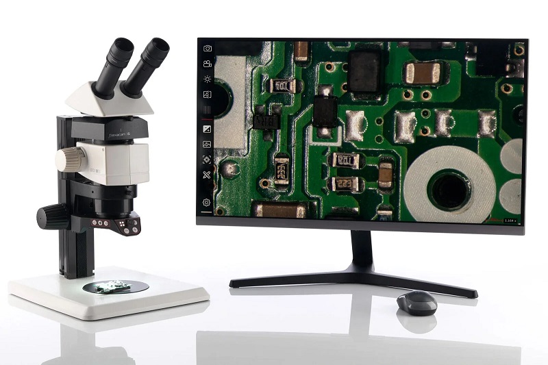
What are the Consideration of Camera PCB Design for Microscope Camera?
The camera PCB design for a microscope camera prioritizes high fidelity and low noise to ensure accurate scientific or medical imaging.
- Low-Noise Power Delivery: A very clean and stable power supply is critical. This involves careful decoupling, using linear regulators or low-noise LDOs instead of switching regulators near the analog sections of the camera sensor PCB.
- Signal Integrity for High Resolution: The data paths from the sensor to the processor must be designed with controlled impedance and length matching to preserve signal integrity, especially for sensors with high pixel counts.
- Thermal Management: Long exposure times can cause sensor heating, introducing noise. The PCB design must incorporate thermal relief vias and consider the overall thermal dissipation path.
- EMI/EMC Considerations: The design must minimize electromagnetic interference to avoid contaminating the sensitive analog signals and to meet regulatory standards. Beyond the electrical design itself, global markets often require additional compliance, such as KC certification for Korea, CE for Europe, or FCC for the United States. These certifications influence grounding strategy, stack-up choices, shielding methods, and material selection. EBest Circuit (Best Technology) has supported customers targeting different regional markets and can adjust the camera PCB design to align with the specific certification framework required for each application.
A well-executed design is paramount for a microscope camera to produce clear, accurate, and reliable images for analysis.
How Does Camera Sensor PCB Selection Influence Camera PCB Board Performance?
The camera sensor PCB is the heart of the imaging system, and its selection dictates the performance envelope and design parameters of the entire camera PCB board.
- Interface and Speed: The sensor’s output interface (e.g., MIPI CSI-2, parallel, LVDS) and data rate determine the required trace routing strategy (impedance control, length matching) on the PCB. Higher speeds demand more sophisticated materials and layout.
- Power Requirements: The sensor’s voltage requirements (e.g., 3.3v, 1.8v, analog 2.8v) define the power delivery network (PDN) complexity on the board. Multiple power domains require careful planning.
- Package and Footprint: The sensor’s package (e.g., BGA, CSP) dictates the PCB’s layer count and design rules. Fine-pitch BGAs may require HDI technology, increasing cost.
- Pixel Size and Resolution: These factors influence the required processing power on the board and the data bandwidth, affecting the choice of main processor and memory.
In short, the camera sensor PCB is the primary driver for the camera PCB board’s architecture, material selection, and overall performance capabilities.
Where to Buy Camera PCB Board?
You can buy camera PCB board from several sources, depending on your needs:
- Original Equipment Manufacturer (OEM): For large-volume production of a custom design.
- Specialized PCB Manufacturers (like BEST Technology): Ideal for prototypes, low-to-medium volume production, and custom designs. They offer full support from design to assembly.
- Component Distributors/Online Marketplaces: For generic PCB camera modules or development boards & kits for hobbyists or prototyping. This is a common source for a camera PCB board for sale as a standard module.
- Supplier for camera PCB board under $100: This is usually only feasible for standard, low-complexity modules bought in volume or simple single-board computers with camera interfaces.
Why Choose EBest Circuit (Best Technology) to Support Your PCB Board Camera Project?
I. Full Expertise and Comprehensive Turnkey Solutions
- 19+ Years of Proven Experience: With a foundation dating back to 2006, EBest Circuit (Best Technology) has nearly two decades of specialized knowledge in advanced Camera PCB manufacturing and assembly.
- Full Turnkey Service: We simplify your supply chain by managing the entire process from camera PCB design to completion—including camera circuit board design, fabrication, component sourcing, assembly (SMT & THT), and final box-build integration.
- One-on-One Expert Support: Dedicated engineering sales and support teams provide personalized service, ensuring your project requirements are meticulously followed.
II. Advanced Manufacturing Capabilities for High-Precision Boards
Board cameras often require compact, high-density, and reliable PCBs. Our capabilities are perfectly suited for these demands:
- High-Density Interconnect (HDI): We support advanced processes like laser blind vias down to 0.10mm and fine trace/space down to 2/2 mil (0.05/0.05mm) for complex, miniaturized designs.
- Advanced Materials: Expertise in various materials, including high-Tg FR4 (for thermal stability), high-frequency materials (Rogers, Taconic for signal integrity), and specialized substrates like ceramic or Metal-Core PCBs (MCPCBs) for thermal management.
- Complex Board Structures: Capability to produce multi-layer boards up to 32 layers, rigid-flex designs, and boards with challenging aspect ratios up to 10:1.
- Diverse Surface Finishes: Offer a wide range of finishes like ENIG, ENEPIG, Immersion Silver, and OSP, which are critical for the reliable soldering of fine-pitch camera sensors PCB and camera parts PCB board.
III. Rigorous Quality Assurance and Certifications
- Certified Quality Management: Adherence to international standards including ISO 9001, ISO 13485, IATF 16949, AS9100D, UL, REACH, and RoHS, ensuring reliability for critical applications.
- Comprehensive Testing: In-house testing facilities include Automated Optical Inspection (AOI), X-Ray inspection for BGAs, flying probe/universal E-testing, micro-section analysis, and functional testing to guarantee flawless performance.
- IPC Standards Compliance: All boards are manufactured and assembled following strict IPC guidelines to ensure high product quality and longevity.
IV. Speed, Flexibility, and Competitive Value
- Rapid Prototyping and Delivery: We understand time-to-market pressures. We offer expedited services, with urgent PCB prototypes shipped within 24-48 hours and PCBA lead times as short as 1-2 days.
- No Minimum Order Quantity (MOQ): Ideal for prototyping and small-to-medium volume production runs, providing flexibility without cost penalties.
V. Dedicated Support for Innovation and Complex Requirements
- Engineering Expertise: Our team has extensive experience with special technologies such as heavy copper (up to 20 oz), impedance control, and extra-thin PCBs (down to 0.15mm), ready to assist with Design for Manufacturability (DFM) feedback.
- Focus on Customer Success: We aim to build long-term partnerships, offering customized solutions and ensuring complete satisfaction with a 97% on-time delivery rate.
In a nutshell, for a PCB board camera project demanding high precision, reliability, and fast time-to-market, EBest Circuit (Best Technology) provides an ideal partnership. Our end-to-end turnkey service, advanced technical capabilities, and unwavering commitment to quality ensure your project is in expert hands from camera PCB design, prototype, fabrication, full assembly to delivery.
All in all, camera PCB board is the critical infrastructure that determines the success of any imaging device. This guide has explored the journey of a camera PCB, from its fundamental role and camera PCB design considerations to cost factors and sourcing.
Navigating the path from a prototype to a reliable, fully assembled camera requires a partner with deep technical expertise and manufacturing precision. BEST Technology excels in producing high-quality, reliable PCBs for all camera applications, from simple security camera boards to advanced DSLR camera PCB boards. We are committed to providing solutions that meet your exact specifications, budget, and timeline. For a consultation or quote, please contact us at sales@bestpcbs.com.
Tags: Camera PCB Board, camera pcb circuit board, dslr camera pcb board