

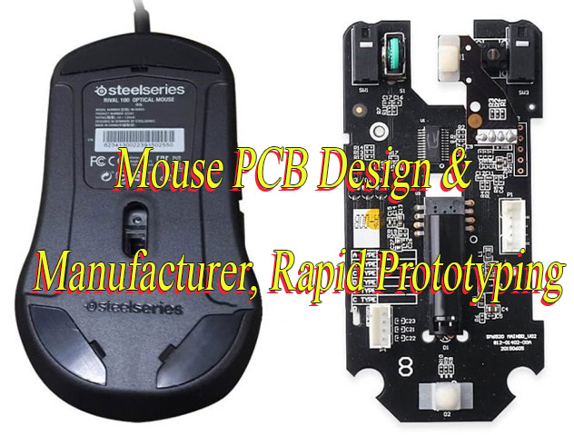
How to design a mouse PCB? Let’s discover definition, parts, function, types, design guide, production process for mouse PCB.
Are you worried about these questions?
- How to cost-effectively mitigate high-frequency signal crosstalk causing cursor jitter?
- With urgent projects, how to achieve 72-hour prototyping from design to validation?
- How to ensure batch-to-batch performance consistency amid quality fluctuations?
As a mouse PCB manufacturer, EBest Circuit (Best Technology) can provide you service and solutions:
- 19-Year Process Database Empowerment – Leverage intelligent defect analysis to deliver impedance matching + ground plane segmentation solutions, cutting high-frequency interference costs by 20%!
- 24-Hour Rapid Prototyping + Free DFM Review – Pre-identify pad spacing/trace width risks to halve prototype cycles, seizing market opportunities ahead of competitors!
- Triple Quality Control System – Full coverage of AOI/X-ray/functional testing integrated with ISO 19001 process controls, achieving <3% batch performance variation for reliable mass production!
Welcome to contact us if you have any request for mouse PCB: sales@bestpcbs.com.
What Is a Mouse PCB?
The mouse PCB is a printed circuit board that carries the core electronic components and serves as the hardware hub of the mouse. It integrates components such as a microcontroller, optical sensor, micro switch, and scroll wheel encoder to convert physical operations (movement/click/scrolling) into digital signals, which are then processed and transmitted to the computer via a wired or wireless interface to achieve cursor control and interactive functions.
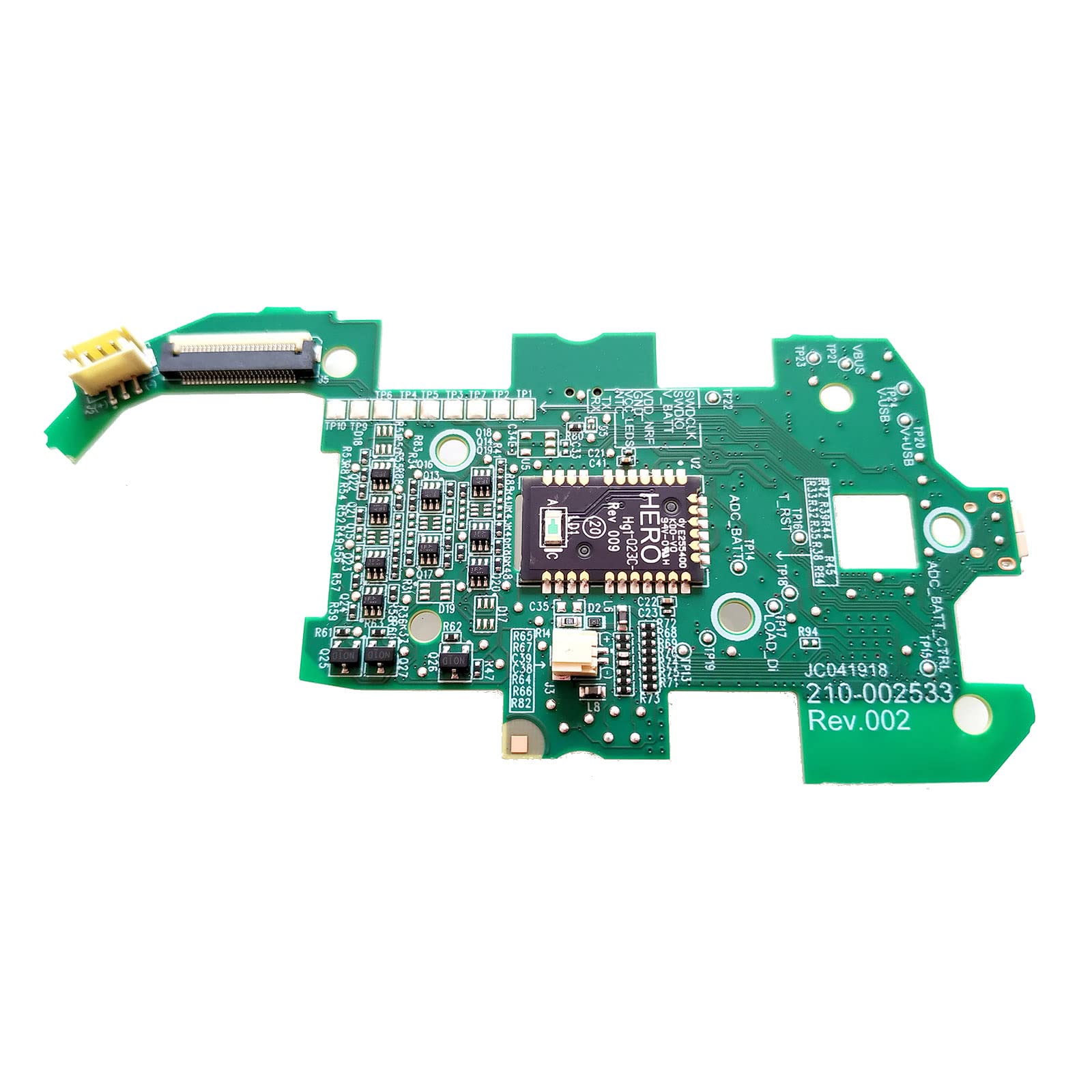
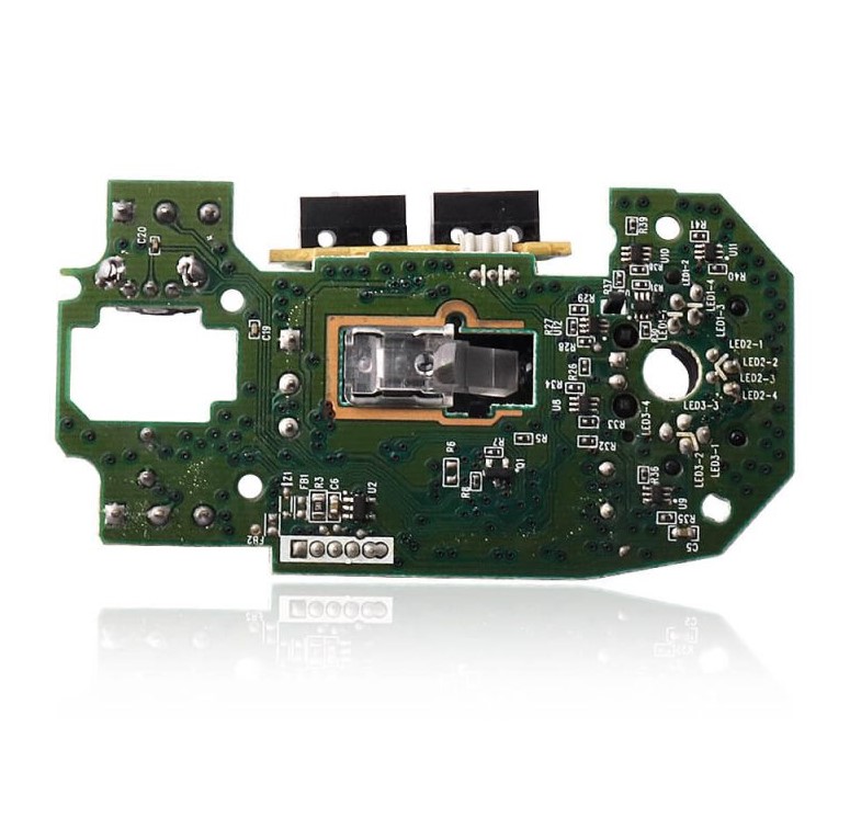
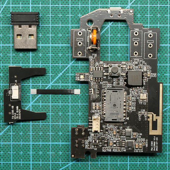
What Are Parts of Mouse PCBs?
Components of Mouse Printed Circuit Board:
- Main Control MCU (Microcontroller): Processes sensor data, executes firmware instructions, manages communication protocols (e.g., USB/HID), and controls peripheral devices.
- Optical Sensor: Core positioning component (e.g., PAW series from PixArt), captures surface textures via CMOS imaging, calculates displacement trajectories, and outputs coordinate data.
- Micro Switch: Mechanical contact electronic switch (typical model: Omron D2FC-F-7N), converts physical clicks into electrical signals to trigger key responses.
- Encoder (Scroll Wheel Module): Mechanical or optical rotary sensor that converts physical scroll wheel rotations into digital pulse signals (e.g., TTC Gold Wheel Encoder).
- Wireless Module (Exclusive to Wireless Mice): Integrates 2.4GHz RF chips (e.g., Nordic nRF52 series) or Bluetooth modules for low-latency data transmission and communication with receivers.
- Power Management Unit: Lithium battery charging ICs (e.g., TI BQ series) and voltage regulation circuits, providing required voltages for components while optimizing wireless mouse battery life.
- Passive Components: Resistor, capacitor, and inductor arrays for signal conditioning, power decoupling, and high-frequency circuit impedance matching (e.g., MLCC capacitors for noise filtering).
- LED Driver Circuit: RGB lighting control chips (often integrated into the MCU), driving multi-zone programmable LEDs for dynamic lighting effects.
What Are Function of PCB Mouse?
Below are Functions of PCB Mouse:
- High integration and compact layout: Unify all components (MCU, sensors, switches, encoders, LEDs, connectors, passives, wireless modules) on a single platform with stable electrical connections, enabling miniaturized and lightweight design.
- Precise signal collaborative processing: Synchronously capture movement signals from optical sensors/roller encoders, click signals from micro-switches, and scroll signals from wheel encoders. Process via MCU for vector calculation, action recognition, DPI switching, and lighting control, then output processed data through wired/wireless channels.
- Efficient power management: Distribute power from USB/battery to all components via voltage regulation and filtering circuits, ensuring stable operation and extending battery life while protecting sensitive elements.
- Firmware extensibility: Store firmware in built-in/external SPI Flash for dynamic function updates (DPI expansion, light effects, protocol optimization), enhancing maintainability and long-term value.
- Multi-mode connectivity: Support USB Type-C/Type-A physical interfaces and wireless antenna interfaces (Bluetooth/2.4GHz), ensuring compatibility with both wired high-speed transmission and stable wireless communication.
- Customizable lighting control: Integrate LED driver circuits (MCU-embedded or standalone) and RGB LED pads for user-defined effects (breathing, gradients, game sync), balancing aesthetics with energy efficiency.
- Modular expandability: Standardized solder pads and interfaces allow modular replacement/upgrades of sensors and wireless modules, extending product lifecycle and meeting personalized performance/function needs.
What Are Types of Mouse PCB Board?
By High-Density Technology Trends
- Multi-layer Rigid-Flex PCB: Adopts 4-layer or higher stacked structures, combining rigid support with flexible connections. Suitable for modular designs (e.g., Razer Viper Ultimate’s “main board + secondary board + display” structure), enabling high-density routing and signal isolation. Meets demands of premium gaming mice for multi-button, RGB lighting, and macro programming.
- HDI (High Density Interconnector) Board: Achieves high integration via microvias, blind/buried vias. Applied in compact devices (e.g., Logitech G Pro X Superlight), supporting native 5000-20000 DPI optical sensors (e.g., PixArt PAW series) and high-speed protocols like USB 3.0.
- RF PCB: Uses low-loss dielectrics like PTFE or Rogers materials, ideal for wireless mouse RF modules (e.g., 2.4GHz antennas) to ensure signal integrity and noise immunity.
By Heat Dissipation and Lightweight Requirements
- Aluminum/Metal Core PCB: High thermal conductivity (1-3W/m·K), used in high-power wireless mice (e.g., Razer Basilisk Ultimate) to extend battery life and enhance structural strength.
- Ceramic Substrates: Ultra-high thermal conductivity (Al₂O₃: 24W/m·K), applied in high-precision optical sensor modules to maintain stability during high-speed computation.
By Application Scenarios and Functional Expansion
- Office Mouse PCB: Uses single/double-layer FR-4 substrate, integrating low-power sensors (e.g., 5000 DPI optical engines) and basic buttons. Supports multi-surface recognition (glass, wood desks) with emphasis on portability and cost efficiency.
- Gaming Mouse PCB: Adopts multi-layer design with high-DPI sensors (e.g., PMW3389, 16000 DPI), programmable buttons, RGB lighting, and macro programming (e.g., MSI DS102 RGB’s 18 RGB LEDs and light guide strip for dynamic effects).
How to Design a Mouse PCB?
Below is a Guide to Mouse PCB Design:
1. Functional Requirements & Specifications Definition
- Define parameters: wired/wireless mode, DPI range (e.g., 100-26,000 DPI), key count (left/right/side buttons, DPI toggle), RGB lighting support, battery life (if wireless), and connectivity standards (USB 2.0/3.0, Bluetooth 5.x/2.4GHz).
- Specify mechanical constraints: PCB dimensions (based on mouse shell), mount points, key switch footprints, sensor window alignment (for optical sensors), and connector placement (USB-C/Type-A).
2. Component Selection & Bill of Materials (BOM)
- MCU Selection: Optimize for ARM Cortex-M4/M7 with hardware accelerators (e.g., NXP LPC55S69 or STM32F4 for DSP instructions). Prioritize GPIO density (≥30 pins), PWM channels (for LED dimming), and integrated peripherals (USB FS/HS, SPI, I²C, ADC for battery monitoring).
- Sensors: Optical sensors like PixArt PMW3395 (26,000 DPI, 50g acceleration) or mechanical encoders (e.g., Alps EC11 for scroll wheel). Include gyroscopes/accelerometers for motion tracking in advanced designs.
- Power Management: Use low-dropout regulators (LDOs) like TPS7A4500 for 3.3V rails, and buck converters (e.g., TPS62840) for efficient 1.8V/1.2V supplies. Include battery fuel gauges (MAX17048) and protection ICs (DW01A for over-current/short-circuit).
- Connectivity & Wireless: USB-C controllers (FUSB302) with CC logic, wireless modules (Nordic nRF5340 with 2.4GHz/BLE 5.3), and antenna matching networks (π-network for 50Ω impedance).
3. Schematic Design & Circuit Partitioning
- Power Rail Design: Implement a 3-stage power tree: input from USB/battery → buck converter → LDOs for noise-sensitive rails. Add decoupling caps (10µF electrolyytic + 100nF ceramic) within 5mm of power pins.
- Signal Paths: Use star topology for digital traces to minimize crosstalk. Separate analog (sensor) and digital (MCU) ground planes with a single-point connection. Implement Schmitt triggers for switch inputs to debounce signals.
- Firmware Interface: Design SPI buses (10MHz) for sensor communication, I²C for auxiliary sensors, and USB HID for configuration. Include a bootloader (e.g., STM32CubeProgrammer) for OTA updates.
- Protection Circuits: Add TVS diodes (SMBJ5.0A) on USB lines, polyfuses for over-current, and ESD suppression (ESD7464) on button pads.
4. PCB Layout & Signal Integrity
- Layer Stackup: Use a 6-layer stack (signal-ground-power-signal-ground-signal). Route USB differential pairs (90Ω impedance) on inner layers with adjacent ground planes. Place sensitive analog traces (sensor data) on top layer with guard rings.
- Component Placement: Cluster the MCU centrally, sensors adjacent to their mechanical windows, and power components near inlets. Orient bypass caps vertically to minimize loop area.
- Signal Integrity: Terminate USB lines with 33Ω series resistors. Use ground stitching vias (0.3mm grid) to connect ground planes. For wireless modules, route antenna traces on microstrip layers with 20mm clearance from digital noise.
- Thermal Management: Add thermal vias under voltage regulators and LED drivers. Use copper pours (70µm) for heat dissipation. Ensure airflow paths for natural convection.
- EMC/EMI Mitigation: Implement ferrite beads on power lines, shield cans for wireless modules, and chokes for high-speed signals. Validate layout against FCC Part 15B/CE RED standards.
5. Firmware & Software Integration
- Firmware Architecture: Use a real-time OS (FreeRTOS) for task scheduling. Implement a state machine for button/sensor handling. Optimize power management with sleep modes (e.g., STM32 Stop Mode with RTC wake-up).
- Storage: Use SPI Flash (Winbond W25Q16JV) for firmware and user profiles. Include wear-leveling and error correction (ECC) for data integrity.
- Configuration Tools: Develop a GUI (Qt/C#) for DPI tuning, lighting effects, and macro programming. Support USB HID and wireless APIs (nRF5340 SDK).
6. Testing & Validation
- Functional Testing: Use a USB protocol analyzer (e.g., Total Phase Beagle) for HID traffic. Validate sensor accuracy with a motion test rig. Measure button response time with an oscilloscope.
- Signal Integrity: Perform TDR/TDT measurements for impedance control. Use a vector network analyzer for S-parameters. Validate eye diagrams for USB 3.0 compliance.
- Power & Thermal: Measure voltage margins with a multimeter. Use thermal cameras to identify hotspots. Validate battery life with a cycle tester.
- EMC/Compliance: Test radiated emissions with a spectrum analyzer. Perform ESD testing (IEC 61000-4-2) and surge testing (IEC 61000-4-5).
- Durability & Reliability: Conduct vibration testing (MIL-STD-810G), drop testing (1.5m to concrete), and thermal cycling (-40°C to 85°C).
7. Manufacturing & Assembly
- DFM/DFA: Use a 2×2 panel with tooling strips. Include fiducials (0.5mm diameter) for pick-and-place. Optimize pad sizes for solderability (ENIG finish).
- Material Selection: FR-4 with Tg 170°C for thermal stability. Use high-CTI substrates for safety compliance.
- Assembly Process: Use SMT for 01005/0201 passives and BGA/QFN packages. Manual assembly for switches/connectors. Perform AOI and X-ray inspection.
- Quality Control: Implement in-circuit test (ICT) for shorts/opens. Conduct functional testing (FT) for all features. Perform burn-in testing (72 hours at 60°C).
How to Make a Mouse PCB Board?
1. Circuit Design Phase
- Schematic Design: Utilize EDA software (e.g., Altium Designer, KiCad) to draft the mouse circuit schematic, defining electrical connections for modules like key matrix, optical sensor, microcontroller, and power management. Annotate component parameters (e.g., resistance, capacitance) and package dimensions (e.g., 0603, SOP-8).
- PCB Layout Design: Route the PCB based on the schematic, prioritizing signal integrity (e.g., differential pair length matching, impedance control), electromagnetic compatibility (avoiding high-frequency signal crosstalk), thermal design (heat sink placement), and manufacturability (minimum trace width/spacing ≥0.1mm, via size ≥0.3mm).
- Gerber File Generation: Output Gerber files (copper layers, solder mask, silkscreen) and Excellon drilling files for subsequent fabrication.
2. Substrate Material Preparation
- Material Selection: FR-4 epoxy glass cloth substrate (thickness 1.6mm±0.1mm) with 35μm copper foil (single/double-sided). Verify flatness, copper adhesion, and dielectric constant (typically 4.2–4.8).
- Cutting & Cleaning: Cut bulk substrate into standard sizes (e.g., 100mm×100mm). Ultrasonic clean to remove contaminants, ensuring process adhesion.
3. Imaging (Pattern Transfer)
- Dry Film Lamination: Apply photosensitive dry film (≈30μm thickness) to cleaned substrate via hot roll lamination, ensuring no bubbles or wrinkles.
- Exposure & Development: Use laser photoplotters to generate artwork from Gerber files. UV exposure (365nm, ≈150mJ/cm²) followed by sodium carbonate development to remove unexposed film, forming etch-resistant circuit patterns.
4. Etching & Stripping
- Etching Process: Spray copper chloride etchant (250–350g/L, 45–55°C) to remove exposed copper, forming precise circuits. Control etching time (2–3 minutes) to prevent over/under-etching.
- Stripping Treatment: Remove residual dry film with sodium hydroxide solution (3–5%), rinse, and dry.
5. Drilling & Plating
- Mechanical Drilling: CNC drilling per Excellon files (hole size 0.3–0.8mm), ensuring smooth burr-free walls.
- Copper Plating: Deposit conductive layer (≥0.5μm) via electroless copper, then electroplate to thicken (≥20μm) for interlayer connectivity. Acid clean to remove oxides.
6. Solder Mask & Surface Finish
- Solder Mask Application: Screen-print liquid photoimageable solder mask (20–30μm thickness) to protect non-soldered areas from oxidation and shorts.
- Silkscreen Printing: Add component identifiers, polarity marks, etc., via white silkscreen for assembly reference.
- Surface Treatment: Apply HASL (hot air solder leveling), ENIG (electroless nickel immersion gold), or OSP (organic solderability preservative) to enhance pad solderability and oxidation resistance.
7. Profiling & Testing
- CNC Profiling: Cut PCB outlines via CNC milling to design specifications (edge smoothness, dimensional tolerance ±0.1mm).
- Electrical Testing: Use flying probe or fixture testing to verify continuity, shorts, and impedance.
- Functional Verification: Assemble critical components (e.g., microcontroller, buttons) for real-world testing of cursor movement, button response, etc.
8. Packaging & Quality Inspection
- Final Inspection: Visual check for defects (solder mask, silkscreen, edges).
- ESD-Safe Packaging: Use antistatic bags to prevent electrostatic damage during transit. Label with batch number, production date, and quality grade.
How to DIY a Mouse PCB Board?
1. Circuit Design & Component Selection
- Use KiCad or Altium Designer to draw circuit schematics, integrating core components including a microcontroller (e.g., STM32 series), optical sensor (e.g., PixArt PAW3360), micro switches, and USB-C interface. Prioritize sensor data line routing to minimize signal delay, and generate Gerber files for PCB manufacturing.
2. PCB Layout & Impedance Control
- Position the optical sensor at the geometric center of the board to reduce offset errors. Surround micro switch pads with grounded copper foil to absorb arc interference. High-speed data traces must maintain equal length and achieve 50Ω impedance matching, avoiding right-angle bends.
3. Substrate Selection & Pattern Transfer
- Select a 1.6mm-thick FR4 double-sided copper-clad laminate. Transfer circuit patterns via thermal transfer or photoengraving. For photoengraving, cover the board with negative film and expose it under UV light for 60-90 seconds to harden traces; unexposed areas are removed using developer solution.
4. Precision Etching & Copper Treatment
- Etch exposed copper with ammonium persulfate solution (1:8 concentration) at 50°C, agitating continuously to accelerate the reaction. After etching, neutralize with sodium carbonate solution, polish the surface, and apply rosin-alcohol solution for oxidation protection.
5. Drilling & Pad Reinforcement
- Drill 0.8mm holes at micro switch pin positions using carbon steel bits, then deburr holes with fine sandpaper. Pre-tin pads using a soldering iron at 350°C to prevent oxidation and enhance soldering reliability.
6. Soldering & Functional Testing
- Solder components in sequence: STM32 chip (preheat to prevent cold joints), sensor, micro switches, and USB interface. Power on and test key response rates using open-source firmware (e.g., QMK). Measure sensor supply voltage fluctuations with a multimeter (target: 3.3V±5%).
7. Structural Adaptation & Case Fabrication
- Model a 3D-printed case based on PCB dimensions, with a 15°-20° thumb rest angle for ergonomic design. Add 0.5mm clearance around micro switch mounts to prevent key sticking. Attach Teflon feet to the base for smooth movement.
Why Choose EBest Circuit (Best Technology) as Mouse PCB Manufacturer?
Reasons Why Choose Us as Mouse PCB Manufacturer:
- Precise Cost Optimization Solutions: Leveraging 19 years of mouse PCB production data to recommend material substitutions and layout optimizations, achieving 15%-30% BOM cost reduction. This directly enhances project profitability and supports budget-sensitive product development.
- Rapid Prototyping Capability: 24-hour rapid prototyping for urgent orders, paired with free DFM analysis to pre-identify 30+ manufacturing risks. This reduces prototype validation time to one-third of traditional cycles, accelerating product launch and market capture.
- Ultra-Reliable Delivery Performance: 99.2% on-time delivery rate supported by intelligent production scheduling systems, ensuring stable production timelines and minimizing supply chain disruption risks or additional costs from delays.
- End-to-End Quality Control: 100% batch inspection with AOI/X-ray/functional testing triple verification, combined with dual ISO 19001/IATF 16949 certified processes, achieving zero-defect bulk shipments and reducing after-sales repair expenses.
- Cross-Industry Compliance Assurance: Medical-grade certifications and RoHS compliance enable seamless adaptation from consumer electronics to medical devices, meeting global market access requirements and enhancing product versatility and competitiveness.
- Process Expertise from Accumulated Experience: 19 years of vertically integrated manufacturing experience with a database of 2,000+ mouse PCB cases provides proven process parameters and risk forecasting, shortening new project ramp-up time and lowering learning costs.
- Customizable Surface Finish Options: Offering HASL/ENIG/OSP and other surface treatment choices to precisely match welding requirements and cost targets, balancing performance with optimal cost efficiency.
Welcome to contact us if you have any request for mouse PCB: sales@bestpcbs.com.
Tags: mouse PCB, mouse PCBs