

High purity alumina (HPA) is a premium ceramic material defined by an aluminum oxide (Al₂O₃) content of 99.99% or higher. This article dives deep into what makes this substance so special and why it’s indispensable for creating the advanced ceramic circuit boards that power our world.
Which of these heat management hurdles is limiting your next-generation electronics design?
- Your circuit boards can’t dissipate heat fast enough, leading to premature device failure.
- You need a substrate material that offers excellent electrical insulation under high voltages.
- You’re struggling to find a base material that remains stable and reliable in extreme temperatures.
- Your designs require a fine-line circuitry that traditional materials can’t support.
- You need a manufacturing partner who can guarantee the quality and consistency of your core substrates.
At EBest Circuit (Best Technology), we specialize in transforming the exceptional properties of high purity alumina into robust ceramic PCBs that directly solve these problems. Here’s how we address each challenge:
- We use high-grade HPA substrates with superior thermal conductivity to efficiently pull heat away from sensitive components.
- Our ceramic PCBs provide outstanding electrical insulation, ensuring safety and performance in high-power applications.
- The inherent thermal stability of alumina ensures your circuits perform reliably even in harsh operating environments.
- Our advanced manufacturing processes allow for precise, high-density circuits on a very stable base.
- Our strict quality control systems, from raw material inspection to final testing, ensure every board meets your exact specifications.
EBest Circuit (Best Technology) is a specialized manufacturer of ceramic PCBs. We are not a producer of high purity alumina powder. Instead, we are experts at engineering this superior material into high-performance circuit boards. Our strength lies in our advanced fabrication processes and commitment to quality, backed by certifications like ISO9001, IATF16949, and AS9100D. If you are looking for a reliable partner to bring your most demanding electronic projects to life, contact us at sales@bestpcbs.com.

What Is High Purity Alumina and Why It Matters in Electronics?
High purity alumina is defined by an exceptional purity level of 99.99% aluminum oxide (Al₂O₃) or higher. This “four-nines” purity is the key that unlocks its superior properties.
But why does such extreme purity matter in electronics? The answer is simple: consistency and performance. Even tiny impurities can act as flaws, disrupting critical characteristics like thermal conductivity and electrical insulation.
To put it simply, using high purity alumina in electronics is like using a perfectly smooth, high-quality canvas for a detailed painting. Any imperfection in the canvas would ruin the final masterpiece. Similarly, HPA provides a flawless foundation for circuits that must be reliable, efficient, and powerful.
| Feature | Why It Matters |
|---|---|
| High Purity (99.99%+) | Ensures consistent and predictable electrical and thermal performance. |
| Excellent Insulator | Prevents electrical leakage and short circuits, even under high voltage. |
| Thermal Conductor | Efficiently draws heat away from sensitive components, preventing overheating. |
| Mechanically Strong | Provides a rigid, stable platform that resists warping and cracking. |
What Is High Purity Alumina Used For?
The applications for high purity alumina are surprisingly wide-ranging. It’s a versatile material that enables progress across several high-tech industries. Its primary uses include:
- LED Lighting: It serves as the base substrate for synthetic sapphire crystals, which are used to make the cores of bright, efficient LED lights.
- Lithium-Ion Batteries: It is used to create fine ceramic coatings on battery separators. This greatly enhances safety by preventing short circuits.
- Semiconductor Processing: It is found in critical chamber components inside semiconductor manufacturing equipment. Its purity prevents contamination of delicate silicon wafers.
- High-Performance Windows: Its scratch-resistant properties make it ideal for watch glasses and smartphone camera lenses.
But from our perspective, one of the most critical uses is in electronics packaging. In the electronics industry, high purity alumina is rapidly becoming the material of choice for thermal management solutions in high-power circuits. When shaped into a circuit board substrate (often called Al₂O₃ PCB), it becomes the backbone of devices that demand superior performance.
What Is the Demand for High Purity Alumina?
The high purity alumina market is not just growing—it’s booming. This growth is fueled by several major technological shifts that all rely on HPA’s unique capabilities. Let’s look at the key drivers:
- The Electric Vehicle (EV) Revolution:
- Application: Lithium-ion battery coatings and power electronics.
- Impact: EVs require safer batteries and efficient power management systems, both of which use HPA. This creates massive demand.
- Proliferation of LED Lighting:
- Application: Substrates for synthetic sapphire crystals used in LED manufacturing.
- Impact: As energy-efficient LED lighting becomes the global standard, demand for HPA remains strong.
- Advancement of Consumer Electronics:
- Application: Semiconductor processing components and thermal management solutions.
- Impact: As smartphones and other devices become more powerful, they generate more heat. HPA-based solutions are critical for heat dissipation.
This rising demand directly influences the high purity alumina price per ton, reflecting its critical role in modern technology. The trend is clear: as the world pushes for more advanced and efficient electronics, the need for high-performance materials like HPA will only increase.
How Is High Purity Alumina Made?
Producing HPA is a meticulous process focused on purifying raw aluminum sources. While the chemistry is complex, the goal is straightforward: remove all impurities to achieve a fine, consistent, and ultra-pure powder. The main production routes include:
- Hydrolysis of Aluminum Alkoxides: This method is known for producing the highest purity levels, often used for ultra high purity alumina.
- Thermal Decomposition of Ammonium Aluminum Sulfate: Another common method that yields high-quality HPA suitable for many electronic applications.
For us at EBest Circuit (Best Technology), the specific high purity alumina production process is secondary to the outcome. We focus intensely on the material’s final properties. The quality of the high purity alumina powder we receive is paramount, as it dictates the performance of our ceramic PCBs.
Our Quality Checkpoint:
Before any alumina substrate enters our production line, we verify its key properties. This ensures the material meets the strict standards required for reliable electronics. The entire high purity alumina production chain must be controlled to deliver a product you can trust.
Why Ceramic PCBs Depend on High Purity Alumina Substrates?
This is the core of the matter. Why is high purity alumina so fundamental to what we do? The answer lies in its unique set of properties that are perfectly suited for demanding electronic applications.
- Superior Thermal Conductivity: Heat is the enemy of electronics. High purity alumina acts like a heat sink, efficiently drawing thermal energy away from sensitive components like power amplifiers and LEDs. This prevents overheating and extends the product’s lifespan.
- Excellent Electrical Insulation: Despite conducting heat well, it is an excellent electrical insulator. This allows it to safely separate high-voltage circuits, a critical requirement in power electronics and automotive applications.
- High Mechanical Strength: Ceramic substrates are robust and rigid. They resist bending and cracking, providing a stable platform for surface-mounted components, even in environments with vibration.
- Chemical Stability: Alpha high purity alumina is highly resistant to corrosion from acids, alkalis, and other harsh chemicals. This makes it ideal for medical, aerospace, and industrial uses.
- Thermal Expansion Match: Its coefficient of thermal expansion is close to that of silicon. This reduces stress on the critical connections between a chip and the board, enhancing reliability.
At EBest Circuit (Best Technology), we work with various grades of alumina, including 96% and the superior 99.6% high purity alumina. For the most extreme thermal challenges, we also offer boards made from Aluminum Nitride (AlN), another advanced ceramic. The choice of material depends entirely on the application’s specific needs for thermal performance and cost.
EBest Circuit (Best Technology) – Turning High Purity Alumina into Reliable Ceramic PCBs
We are the crucial link in the chain. Our role is to take this exceptional raw material and engineer it into a functional, high-performance circuit board. This transformation requires specialized expertise and technology.
- Advanced Manufacturing: We employ state-of-the-art processes like laser drilling for precise micro-vias and Direct Plated Copper (DPC) for creating fine circuit patterns directly on the ceramic.
- Rigorous Quality Systems: Our ISO certifications (including IATF 16949 for automotive and AS9100D for aerospace) are not just certificates. They represent a deep commitment to quality that is embedded in every step of our production.
- Full Traceability: Our Manufacturing Execution System (MES) tracks every board throughout production. This ensures complete traceability and allows for 100% electrical testing before shipment.
In short, EBest Circuit (Best Technology) is not a high purity alumina producer. We are a solution provider. We master the process of converting ultra high purity alumina substrates into reliable, high-performance ceramic PCBs that meet the precise demands of your application.
Why Global Clients Choose EBest Circuit (Best Technology) for Ceramic PCB Manufacturing?
Global clients partner with us because we deliver more than just a component; we deliver reliability. They choose EBest Circuit (Best Technology) for three key reasons:
- Technical Expertise: Our team understands both the materials and the electronics. We can provide expert guidance on selecting the right substrate and manufacturing process for your project.
- Proven Consistency: Our stringent quality controls mean that the tenth board we ship will perform identically to the ten-thousandth. This consistency is vital for mass production.
- A Partnership Approach: We see ourselves as an extension of your engineering team. We work with you to solve problems and optimize designs for manufacturability and performance.
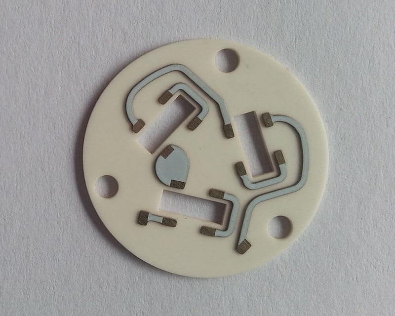
Case of Alumina Ceramic PCB Fabrication by EBest Circuit (Best Technology)
Alumina ceramic PCBs are widely used in various high-reliability and high-performance fields due to our excellent thermal conductivity, high insulation strength, temperature resistance, and chemical stability. Key applications include:
- Power Electronics: IGBT modules, power modules, inverters, etc., for high power density and thermal management.
- RF/Microwave Communication: Base station amplifiers, radar systems, leveraging low dielectric loss and high-frequency stability.
- Automotive Electronics: Especially in electric vehicle battery management systems (BMS) and electronic control units (ECUs), due to high-temperature resistance and vibration tolerance.
- Aerospace and Military: Control systems and sensors requiring high reliability under harsh conditions.
- LED Packaging: Substrates for high-power LEDs, providing efficient heat dissipation.
- Medical Devices: Implantable devices and diagnostic equipment, benefiting from biocompatibility and stability.
- Industrial Controls: Sensors and actuators operating in high-temperature environments.
Key Fabrication Capabilities
Thick Film Technology
- Substrate Materials: Al₂O₃, AlN, BeO
- Maximum Board Size: 50×50mm (0.635mm thickness); 80×80mm (1.0mm thickness)
- Minimum Line Width/Space: 150/150 µm
- Maximum Layers: 4 layers
- Conductor Thickness: AgPd up to 20µm; Au up to 15µm
- Surface Finish: Not required (AgPt/Au directly used)
- Special Capabilities: Resistor tolerance ±0.3% (laser trimmable), wire bondable
Thin Film Technology
- Substrate Materials: Al₂O₃, AlN, Si, etc.
- Maximum Board Size: 50×50mm (0.38mm thickness); 100×100mm (0.5-1.0mm thickness)
- Minimum Line Width/Space: 75/75 µm (can be refined to 20µm)
- Minimum Via Diameter: 0.10 mm
- Maximum Layers: 2 layers
- Conductor Thickness: Au up to 3µm
- Surface Finish: Plating (2-5µm)
- Special Capabilities: High line width accuracy (±5µm), resistor tolerance ±0.1%, wire bondable
LTCC (Low Temperature Co-fired Ceramic)
- Substrate Material: Glass-ceramic composite
- Maximum Board Size: 50×50mm (thickness <1.0mm); 150×150mm (thickness ≥1.0mm)
- Minimum Line Width/Space: 80/80 µm
- Minimum Via Diameter: 0.10 mm
- Maximum Layers: 40 layers
- Conductor Thickness: 6-20 µm
- Surface Finish: Usually not required; optional plated Ni/Pd/Au
- Special Capabilities: Multilayer co-firing, suitable for high-frequency applications (Dk 9.1 @13GHz)
HTCC (High Temperature Co-fired Ceramic)
- Substrate Material: 92% Alumina Ceramic
- Maximum Board Size: 50×50mm (thickness <1.0mm); 150×150mm (thickness ≥1.0mm)
- Minimum Line Width/Space: 150/150 µm
- Minimum Via Diameter: 0.15 mm
- Maximum Layers: 30 layers
- Conductor Thickness: W/MoMn: 6-15µm
- Surface Finish: Plated Ni/Pd/Au (2.5-4µm/0.5µm/0.3µm)
- Special Capabilities: High-temperature sintering (>1600°C), high mechanical strength
General Attributes (Common across all processes)
- Substrate Thickness Range: 0.15mm – 6mm (specific range depends on process)
- Thermal Conductivity: 17 – 170 W/m·K (AlN substrates can reach 170 W/m·K)
- Dielectric Strength: ≥15 kV/mm
- Warpage: <0.3%, suitable for high-precision assembly
- Wire Bonding Support: All processes support Au/Al wire bonding (common wire diameters: 18–50µm)
In conclusion, high purity alumina provides the essential foundation for the advanced electronics that define our modern world. This article has explored its critical role, especially in the creation of high-performance ceramic circuit boards.
EBest Circuit (Best Technology) has the specialized knowledge and manufacturing excellence to turn the potential of high purity alumina into a real-world advantage for your products. Pls feel free to reach out to our team at sales@bestpcbs.com for our ceramic PCB specifications or quotes.
Tags: High Purity Alumina