

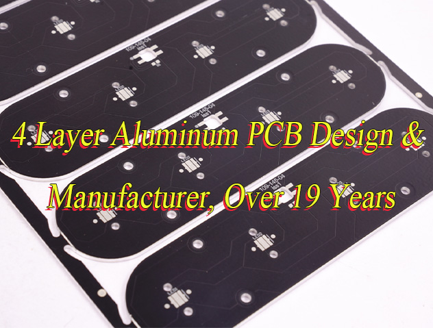
What is 4 layer aluminum PCB? Let’s discover definition, benefits, applications, design spec and guideline, production process for 4L PCB together.
Are you troubled with these issues?
- How does a 4-layer aluminum PCB eliminate thermal overload concerns in high-power LED/power modules?
- How to achieve the perfect balance of high performance and low cost with aluminum substrates?
- How to ensure rapid yet reliable prototyping and mass production with 4-layer aluminum PCBs?
As a 4 layer PCB manufacturer, EBest Circuit (Best Technology) can provide you services and solutions:
- Thermal Breakthrough: 20 years of aluminum process expertise + micro-via thermal conduction patent, boosting thermal dissipation efficiency by 30%, solving FR4 thermal buildup issues.
- Cost Breakthrough: Bulk procurement + intelligent production scheduling, reducing per-board costs by 15-20%, delivering unbeatable value in competitive markets.
- Delivery Breakthrough: 24-hour rapid prototyping + 99.2% on-time delivery, turning time into tangible value.
Welcome to contact us if you have any request for 4 layer aluminum PCB: sales@bestpcbs.com.
What Does a 4 Layer Aluminum PCB Mean?
A 4 layer aluminum PCB is a printed circuit board composed of an aluminum alloy (such as 6061/5052) as the base material, forming a composite structure of “aluminum substrate layer – insulating and thermally conductive layer – multi-layer copper foil layers”.
Its core structure typically includes a 1.5-2.0mm thick aluminum substrate layer (providing mechanical support and efficient heat dissipation), a 30-100μm thick alumina-filled epoxy resin insulating layer (thermal conductivity 1.5-8 W/m·K, combining electrical insulation and thermal conduction functions), and multi-layer copper foil layers (such as 2oz copper thickness heat dissipation layer, 1oz copper thickness signal/power layer).
Why Choose 4-Layers Aluminum PCB Board?
Advantages of 4 layer aluminum PCB board:
- Enhanced Heat Dissipation & Lifespan: High thermal conductivity (1-8W/m·K) with 4-layer structure reduces thermal resistance by over 50%, minimizing overheating risks for high-heat components like LEDs/power modules, extending product life by 30-50% and cutting maintenance costs.
- Lightweight & Cost-Efficient: Aluminum is 1/3 the density of copper; 4-layer boards are 40-60% lighter than copper alternatives, with 1.0-1.6mm thickness maintaining strength. Lowers shipping costs by 20-35%, ideal for weight-sensitive applications like drones/automotive electronics.
- Improved Reliability: Matched thermal expansion coefficient (CTE) with chips reduces solder joint cracking by 40%+ via fiber-reinforced layers, lowering failure rates and boosting end-user satisfaction.
- EMI Shielding & Stability: Natural EMI shielding plus 4-layer ground plane design creates a Faraday cage effect (60-80dB shielding), minimizing signal interference and system errors, reducing debugging costs.
- Cost & Eco-Friendly Benefits: Aluminum costs 1/3 of copper; optimized trace density cuts material use, supporting SMT automation. 20-30% lower BOM costs with 15% higher production efficiency. 100% recyclable, lead/halogen-free process meets RoHS, enhancing ESG compliance.
- Robust Mechanical Performance: 250MPa+ bending strength with fiber reinforcement handles -40°C~150°C temperatures and high-vibration environments (e.g., industrial controls), reducing physical damage risks.
When to Use 4 Layer Aluminum PCB?
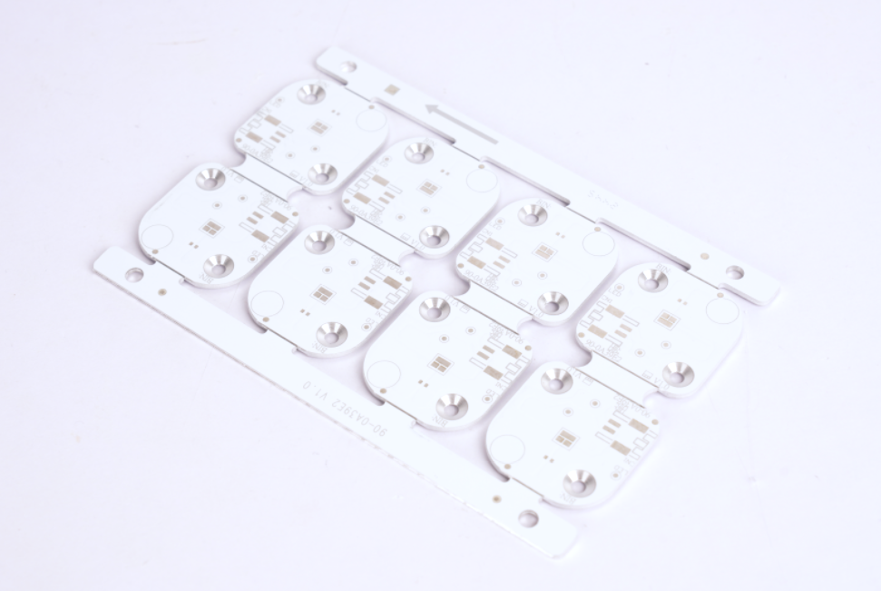
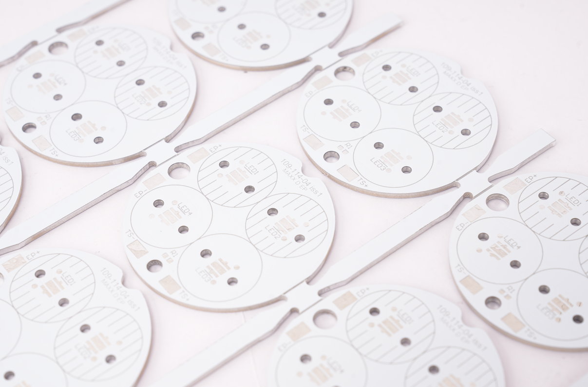
Applications of 4 Layer aluminum PCBs:
- High-Power LED Lighting (e.g., stage lights, grow lights).
- New Energy Vehicle Power Modules (motor controllers, on-board chargers).
- 5G Base Station RF Power Amplifier Units.
- Industrial Servo Drives.
- Medical Imaging Equipment Thermal Management Modules (CT machines, ultrasound probes).
- Aviation Electronics (airborne radars, satellite communication modules).
4 Layer Aluminum PCB Design Specification
| Design Parameter | Typical Value/Range |
| Aluminum Core Type | Thickness 1.0-3.0mm |
| Dielectric Layer Thermal Conductivity | ≥1.5W/mK |
| Layer Stack Sequence | Total Thickness 1.6±0.2mm |
| Copper Thickness Selection | Outer Layer: 1-3oz / Inner Layer: 0.5-2oz |
| Thermal Resistance Calculation | Rθ < 2.5℃/W |
| Thermal Via Design | Hole Diameter 0.3mm / Pitch 1.5mm |
| Insulation Voltage Withstand | ≥3kV(AC) |
| Characteristic Impedance Control | ±10% Tolerance |
| Mounting Hole Position | M3/M4 Standard Hole Size |
| Warpage Control | ≤0.5% of Board Thickness |
| Solder Mask Opening | Opening Size ≥ Component Pad + 0.2mm |
| Surface Finish | ENIG 0.05-0.1μm |
| Thermal Cycling Test | No Delamination/Cracking |
| Insulation Resistance | ≥100MΩ (500VDC) |
4 Layer Aluminum PCB Board Design Guide
A guide to 4 layer aluminum PCB design:
1. Aluminum Core Substrate Selection
- Material Selection Rationale: 6061-T6 aluminum alloy (thermal conductivity: 167 W/mK, tensile strength: 310 MPa) is ideal for high-power applications; 5052 alloy offers superior corrosion resistance for humid environments. Compliance with ASTM B209 ensures material integrity, validated via salt spray testing (ASTM B117) for corrosion resistance.
- Surface Treatment Parameters: Anodizing employs sulfuric acid electrolyte (150–200 g/L) at 15–20 V for 30–45 minutes. Oxide film thickness (15–20 μm) is verified by eddy-current thickness gauge (±2 μm precision). Boiling water sealing ensures insulation resistance ≥100 MΩ (500 VDC).
- Flatness Control Standard: Three-point measurement mandates ≤0.5% board thickness tolerance (e.g., ≤0.008 mm for 1.6 mm boards), validated by laser profilometry with traceable DFMEA documentation.
2. Thermal Dielectric Layer Design
- Material Performance Validation: Thermal conductivity ≥1.5 W/mK is confirmed via laser flash analysis (ASTM E1461). Recommended composite: epoxy resin with 60–70% volume fraction of 5–15 μm alumina filler. Glass transition temperature (Tg ≥150°C) and CTE (≤25 ppm/°C) are verified by DSC and TMA testing, respectively.
- Lamination Process Control: Vacuum hot-pressing at 180–200°C, 3–5 MPa for 90–120 minutes achieves thickness uniformity ≤±5% (X-ray thickness gauge). Adhesion strength ≥0.8 kN/cm is validated by microsection analysis per IPC-TM-650.
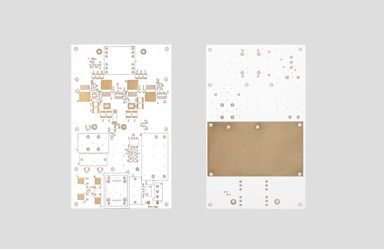
3. Stack-Up Optimization
- Symmetric Layer Design: “Aluminum base–dielectric–copper foil–PP sheet–inner layer–PP sheet–copper foil” symmetry ensures total thickness 1.6 ±0.2 mm. ANSYS thermal simulation confirms warpage ≤0.5% board thickness.
- Drilling Parameters: High-speed drilling uses 0.3 mm tungsten carbide bits at 50,000–60,000 rpm with 0.5–1.0 m/min feed rate. Hole wall roughness ≤25 μm is inspected optically; plasma desmear ensures cleanliness per IPC-6012.
4. Copper Thickness Allocation
- Current Density Calculation: Outer layer 1–3 oz (35–105 μm) follows J=I/(w×t) with ≤4 A/mm² current density. Inner layer 0.5–2 oz (17–70 μm) utilizes pulse plating for localized thickness enhancement.
- Trace Design Rules: Minimum trace/space meets manufacturing capability (e.g., 0.1 mm/0.1 mm). Etch factor ≥2.5 is verified by metallographic microscopy. Differential pair impedance is controlled within ±10% via Polar Si9000 calculations and TDR validation.
5. Thermal Management Solutions
- Thermal Via Arrays: 0.3 mm via diameter/1.5 mm pitch design is thermally validated by Rθ=ΔT/P. Electroplated copper filling achieves ≥95% fill rate, confirmed by cross-sectional analysis.
- 3D Thermal Simulation: ANSYS Icepak models power density ≤5 W/cm², ensuring critical components operate ≤125°C. Post-thermal cycling (-55°C~125°C, 1000 cycles) acoustic microscopy confirms no delamination/cracking.
6. Electrical Performance Assurance
- Dielectric Withstanding Voltage: ≥3 kV AC is ensured by dielectric thickness (≥0.1 mm) and material selection. Hipot testing (3 kV AC, 1 min) confirms no breakdown. Insulation resistance ≥100 MΩ (500 VDC) is validated by pressure cooking (85°C/85% RH, 168 h).
- Impedance Control: ±10% tolerance for characteristic impedance is achieved via differential pair design and TDR verification.
7. Mechanical Enhancement Strategies
- Warpage Mitigation: Symmetric stack-up and stress compensation limit warpage ≤0.5% board thickness. M3/M4 mounting holes feature ≥25 μm plated wall thickness (X-ray inspection).
- Solder Mask Design: Opening size ≥ component pad +0.2 mm is optically measured. LPI solder mask ensures edge smoothness ≤0.1 mm and 20–30 μm thickness (film thickness gauge).
8. Surface Finish Selection
- ENIG Parameters: 3–8 μm nickel (XRF) and 0.05–0.1 μm gold (SEM) layers withstand -40°C~125°C thermal shock (500 cycles) and solderability tests (288°C, 3×10 s).
- Alternative Finishes: OSP suits lead-free soldering (≥260°C tolerance); immersion silver offers high conductivity (≥2×10⁵ S/cm) for RF applications. Selection balances cost and performance.
9. Reliability Verification System
- Thermal Cycling Test: Post-1000-cycle (-55°C~125°C) inspection includes acoustic microscopy and electrical testing.
- Thermal Stress Test: Solder dip (288°C, 3×10 s) followed by microsection analysis (≥0.8 kN/cm adhesion) and dye penetration testing.
10. Manufacturing Process Control
- Drilling Accuracy: X-ray drilling achieves ±50 μm positional accuracy. AOI covers defect detection (shorts/opens, mask defects) per IPC-A-600.
- Lamination Monitoring: Real-time pressure (±5%) and temperature (±2°C) control via sensors. Microsection and dye testing data are logged in MES for traceability.
How to Make a 4 Layer Aluminum Printed Circuit Board?
4-Layer Aluminum PCB Manufacturing Process:
1. Material Preparation & Substrate Pretreatment
- Substrate Selection: Use 6061-T6/5052 aluminum alloy (thermal conductivity: 167/190 W/mK) with 1.0–3.0 mm thickness. Surface undergoes anodizing treatment (oxide film 15–20 μm) and salt spray testing (ASTM B117) for corrosion resistance. Copper foil thickness follows design specifications (outer layer: 1–3 oz; inner layer: 0.5–2 oz) with flatness ≤0.5% board thickness.
- Cutting & Cleaning: Precision cutting to design dimensions followed by ultrasonic cleaning to remove contaminants. Protective film applied to aluminum surface to prevent scratches; gloves mandatory during handling.
2. Inner Layer Core Board Fabrication
- Pattern Transfer: Clean copper-clad laminate, apply photoresist, and transfer circuit patterns via UV exposure (15–20 mJ/cm² energy). Develop and cure photoresist to form protective layer.
- Etching & Stripping: Alkaline etching (e.g., NaOH) removes unprotected copper; line width/spacing verified via metallographic microscopy (etch factor ≥2.5). Photoresist stripped post-etching; circuit integrity checked for opens/shorts.
3. Lamination Process
- Stack-Up Structure: Symmetric “aluminum base–dielectric–copper foil–inner layer–PP sheet” configuration ensures total thickness 1.6 ±0.2 mm. Dielectric layer uses high-thermal-conductivity epoxy resin with ceramic fillers (≥1.5 W/mK); pre-lamination vacuum baking removes moisture.
- Hot Pressing: Vacuum hot press at 180–200°C/3–5 MPa for 90–120 minutes ensures PP sheet fusion. Post-lamination X-ray inspection verifies layer alignment (≤±50 μm); warpage ≤0.5% board thickness via laser measurement.
4. Drilling & Hole Metallization
- Drilling Parameters: Tungsten carbide drill bits (0.3 mm diameter) operate at 50,000–60,000 rpm with 0.5–1.0 m/min feed rate. Plasma desmear cleans hole walls (IPC-6012 compliant).
- Copper Plating: Electroless copper + electroplating forms 25 μm copper layer. TDR testing validates impedance control (±10% tolerance); cross-section analysis confirms ≥95% fill rate.
5. Outer Layer Circuit Fabrication
- Pattern Transfer: Positive photoresist process for outer layers; alkaline etching forms circuits. Tin stripping retains protective layer. AOI inspects line width/spacing compliance.
- Surface Finish: ENIG (3–8 μm nickel/0.05–0.1 μm gold) verified by XRF/SEM. Alternatives include OSP (≥260°C heat resistance) or immersion silver (≥2×10⁵ S/cm conductivity) based on application requirements.
6. Solder Mask & Legend Printing
- Solder Mask Application: LPI solder mask applied via screen printing, pre-baked, exposed, and developed. Edge smoothness ≤0.1 mm; thickness 20–30 μm. Opening size ≥ component pad +0.2 mm ensures solderability.
- Legend Printing: Screen-printed component identifiers with clear, non-overlapping fonts. Cured for adhesion durability.
7. Profiling & Cutting
- V-Cut/Routing: V-Cut separates boards with burr height ≤25 μm. Precision routing ensures dimensional tolerance ≤±0.1 mm. Deburring performed post-cutting.
8. Testing & Inspection
- Electrical Testing: Flying probe tests verify connectivity; AOI detects shorts/opens; X-ray checks layer alignment. Insulation resistance ≥100 MΩ (500 VDC); dielectric strength ≥3 kV AC.
- Reliability Testing: Thermal cycling (-55°C~125°C, 1000 cycles), thermal shock (288°C solder dip ×3), and vibration testing per IPC-6012. Acoustic microscopy confirms no delamination/cracking.
9. Packaging & Shipment
- Cleaning & Packaging: Ultrasonic cleaning removes residues; vacuum packaging prevents moisture ingress. Packaging includes product labels and quality reports (dimensional, electrical, reliability data).
- Final Inspection: Full inspection by FQC and random checks by FQA ensure compliance with customer specifications and industry standards.
Why Choose EBest Circuit (Best Technology) as 4 Layer Aluminum PCB Manufacturer?
Reasons why choose us as 4 layer aluminum PCB manufacturer:
- Cost Optimization Leadership: Leverage 19 years of process expertise and bulk procurement advantages to deliver cost-sensitive design solutions, reducing production costs by 15%-20% versus industry benchmarks while maintaining high performance.
- Certification Compliance: Full spectrum of certifications including ISO 9001, IATF 16949 (automotive), medical-grade approvals, and RoHS compliance, enabling seamless market access across automotive, medical, and consumer sectors.
- Free DFM Support: 19 years of aluminum PCB expertise identifies over 90% of early-stage manufacturability risks via free DFM analysis, reducing rework costs and time
- Reliable Delivery Performance: Achieve 99.2% on-time delivery rate through intelligent production scheduling and end-to-end visibility, minimizing supply chain risks and inventory pressure.
- Strict Quality Inspection: Implement 100% full-inspection with AOI/X-ray systems, achieving defect rates below 0.05% and exceeding industry standards for batch-to-batch consistency.
- Integrated One-Stop Service: Streamline design-prototype-production-testing workflows, cutting client coordination efforts by 40% and enhancing project efficiency from concept to mass production.
- Custom Technical Support: Provide specialized solutions for aluminum PCB thermal management and high-temperature reliability, including thermal simulation and impedance optimization.
- Rapid Response Excellence: Support 24-hour rapid prototyping for urgent orders, cutting development cycles by 50% compared to industry norms and accelerating market entry.
- Sustainable Manufacturing: Adopt eco-friendly processes and materials compliant with RoHS/REACH, supporting global market compliance and eco-certification goals.
Our Multilayer Aluminum PCB Capabilities
| Parameter | Capabilities |
| Base Material | Aluminum Base |
| Thermal Conductivity (Dielectric Layer) | 0.8 W/(m·K), 1.0 W/(m·K), 1.5 W/(m·K), 2.0 W/(m·K), 3.0 W/(m·K) |
| Board Thickness | 0.5mm~3.0mm (0.02″~0.12″) |
| Copper Thickness | 0.5 OZ, 1.0 OZ, 2.0 OZ, 3.0 OZ, up to 10 OZ |
| Outline Processing | Routing, Punching, V-Cut |
| Soldermask Color | White/Black/Blue/Green/Red Oil |
| Legend/Silkscreen Color | Black/White |
| Surface Finishing | Immersion Gold, HASL (Hot Air Solder Leveling), OSP (Organic Solderability Preservative) |
| Max Panel Size | 600mm × 500mm (23.62″ × 19.68″) |
| Packing Method | Vacuum Packaging/Plastic Bag Sealing |
| Sample Lead Time (L/T) | 4~6 Days |
| Mass Production Lead Time (MP) | 5~7 Days |
How to Get a Quote for Multilayer Aluminum PCB Project?
Multilayer Aluminum PCB Project Quote Request:
1. Board Specifications
- Layer Count: 4-layer (specified as aluminum-core).
- Dimensions: Exact PCB size (length × width × thickness).
- Material Type: Aluminum substrate (e.g., Al5052, Al6061) + FR4/epoxy dielectric layers.
- Surface Finish: ENIG, HASL, OSP, or other (specify for solderability/corrosion resistance).
2. Technical Parameters
- Minimum Trace Width/Spacing: Critical for manufacturing precision (e.g., 0.1mm/0.1mm).
- Impedance Control: Required tolerance (e.g., ±10% for RF/high-speed signals).
- Thermal Management Features: Thermal via density, heat sink integration, or copper pour requirements.
3. Production Details
- Order Quantity: Prototype (1-100pcs) / Small batch (100-1000pcs) / Mass production (1000+ pcs).
- Delivery Timeframe: Urgent (3-5 days) / Standard (7-10 days) / Economy (14+ days).
- Special Requirements: Buried/blind vias, edge plating, conformal coating, or RoHS/REACH compliance.
4. Design Files
- Gerber RS-274X files + Drill drawings.
- BOM (Bill of Materials) if applicable.
- 3D STEP models for mechanical fit validation (optional but recommended).
Welcome to submit your Gerber files to us for a quote now: sales@bestpcbs.com.