

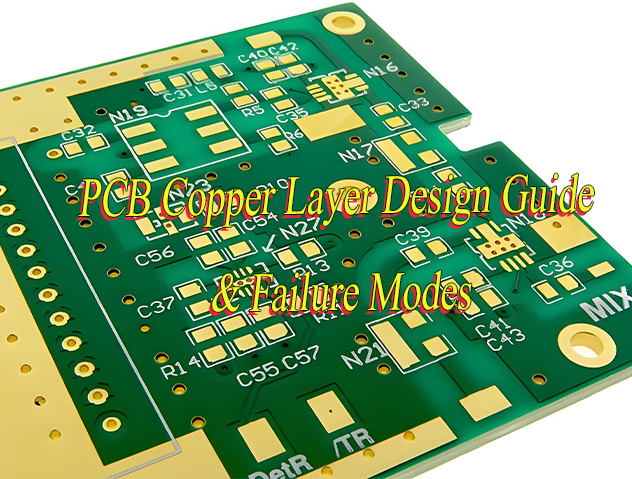
How to design PCB copper layer for copper balancing? Let’s explore meaning, types, functions, design spec, design guide and failure modes for PCB copper layer through this blog.
Are you troubled with these problems?
- Frequent PCB burnout in high-current scenarios? The core issue is insufficient copper layer current-carrying capacity!
- High signal loss and slow transmission in high-speed applications? Poor copper layer uniformity is the bottleneck!
- Excessive device heating and shortened lifespan? Inadequate copper layer heat dissipation is the root cause!
As a PCB manufacturer, EBest Circuit (Best Technology) can provide you service and solutions:
- Copper Layer Current-Carrying Capacity Upgrade: Boost current-carrying capacity by 40% for rock-solid performance under high loads.
- Copper Layer Uniformity Control: Achieve thickness tolerance of ±3%, reducing signal loss by 20% for sharper high-speed performance.
- Thermal Design & Copper Layer Synergy: Enhance heat dissipation efficiency by 15% and extend device lifespan by 30% through optimized copper layer distribution and thermal path alignment.
Welcome to contact us if you have any request for PCB design and manufacturing: sales@bestpcbs.com.
What is PCB Copper Layer?
The PCB copper layer is formed by etching pure copper foil laminated onto an insulating substrate (such as FR-4). Precision-designed traces connect electronic components, solder pads secure device pins, and large copper surfaces provide the combined functions of current conduction, signal transmission, heat dissipation, and electromagnetic shielding.
What Are Types of Copper Layer in PCB?
Types of PCB copper layer:
Signal Layer
- Function: Transmits high-speed digital/analog signals while ensuring signal integrity.
- Features: Utilizes microstrip/stripline structures with optimized impedance matching (e.g., 50Ω/100Ω) and supports differential pairs for noise suppression.
- Applications: High-speed buses (USB/HDMI), RF signals, clock lines.
Power Plane Layer
- Function: Provides a low-impedance power distribution network (PDN) to minimize voltage drops and noise.
- Features: Full-layer copper coverage with optional segmentation into isolated power zones (e.g., VCC/GND), paired with decoupling capacitors for high-frequency noise suppression.
- Applications: Processor power supply, analog circuit bias, high-current loads.
Ground Plane Layer
- Function: Offers a low-impedance reference ground to reduce EMI and serves as a signal return path.
- Features: Continuous copper coverage with multiple via connections to minimize impedance, avoiding segmentation to prevent ground loops.
- Applications: Digital circuit ground, analog circuit shielding, RF grounding.
Shielding Layer
- Function: Isolates sensitive or high-speed signals to prevent interference/crosstalk.
- Features: Mesh or solid copper coverage with grounded vias forming a Faraday cage, optionally integrated with ferrite beads/filters.
- Applications: RF modules, high-speed digital isolation, power supply noise suppression.
Thermal Layer
- Function: Conducts heat away from high-power components via high-thermal-conductivity copper to prevent overheating.
- Features: Solid copper coverage over hotspots with thermal vias for heat dissipation to structures, optionally paired with thermal interface materials.
- Applications: Power transistors, LEDs, processor cooling.
Impedance-Controlled Layer
- Function: Precisely controls trace width/spacing/dielectric thickness to achieve target impedance (e.g., 50Ω).
- Features: Microstrip/stripline design requiring dielectric constant and copper thickness calculations, optionally with termination resistors for impedance matching.
- Applications: High-speed serial interfaces (PCIe/SATA), RF paths, differential pairs.
Hybrid Function Layer
- Function: Integrates multiple functions (e.g., signal+power) to optimize layer count and cost.
- Features: Segmented copper zones for different functions with attention to isolation and signal integrity, optionally embedded with buried resistors/capacitors.
- Applications: High-Density Interconnect (HDI) boards, inner layers of multilayer PCBs.
What Are Functions of PCB Copper Layer?
Functions of PCB copper layer:
- Current Transmission: Forms conductive pathways to efficiently transmit electrical signals and power, ensuring normal circuit operation.
- Thermal Management: Leverages copper’s high thermal conductivity to rapidly dissipate heat generated by components, maintaining stable circuit temperatures.
- Signal Shielding: Acts as a shielding layer to reduce electromagnetic interference (EMI), enhancing signal integrity and noise immunity.
- Impedance Control: Precisely adjusts copper layer width, spacing, and thickness to optimize characteristic impedance of signal transmission lines, ensuring high-speed signal stability.
- Power Distribution: Constructs low-impedance power networks to minimize voltage drops, providing stable power supply to critical components.
- Mechanical Support: Enhances PCB structural rigidity, preventing deformation or fracture caused by external forces or thermal expansion.
- Grounding Design: Offers low-impedance grounding paths to eliminate static charge accumulation, ensuring device safety and stable signal reference.
- Thermal Expansion Mitigation: Mitigates thermal stress-induced damage to the PCB through copper-substrate synergy, extending operational lifespan.
Copper Layer PCB Design Specification
| Parameter Category | Specific Requirements |
| Copper Thickness Selection | 1oz Cu: 4A/mm² (ΔT=10℃) |
| 2oz Cu: 7A/mm² (ΔT=10℃) | |
| 3oz Cu: 12A/mm² (ΔT=10℃) | |
| High-Frequency Loss Control | ≥1GHz signals: Cu thickness ≤0.5oz (18μm) |
| >10GHz: Copper foil roughness ≤1.2μm (RTF copper foil) | |
| Minimum Trace Width/Spacing | 1oz Cu: ≥3mil/3mil; 2oz Cu: ≥5mil/5mil; 3oz Cu: ≥8mil/8mil |
| Impedance Control Tolerance | Single-ended: ±10%; Differential pairs: ±7% ; RF traces: ±3% |
| Shielded Copper Mesh | Void ratio ≤20% (f>1GHz); Ground via spacing ≤λ/10 (λ = minimum wavelength) |
| Thermal Copper Island | Size ≥150% of power device area; Thermal vias: 0.3mm diameter, spacing ≤1.5mm |
| Power-Ground Plane Spacing | ≤4mil (enhanced decoupling); Dielectric thickness tolerance: ±10% |
| Reference Plane Crack Handling | No cracks in high-speed signal reference planes |
| Thick Copper Step Transition | Adjacent layer Cu thickness difference ≥2oz: 30°tapered edge; Minimum transition length ≥10mm |
| Thick Copper Etching Compensation | 3oz Cu: Line width compensation +20%; Sidewall undercut ≤Cu thickness ×0.25 |
| HDI Microvia Layer Copper Thickness | Laser-drilled layers: 0.3oz~0.5oz (9-18μm) ; Line width accuracy: ±0.02mm |
| Copper Foil Adhesion | 1oz Cu/FR4: ≥1.0N/mm; High-Tg substrate: ≥1.2N/mm |
| Thick Copper Thermal Reliability | 3oz+ Cu layers: TG≥170℃ substrate; CTE matching: Cu-CTE ≤18ppm/℃ |
| Current Carrying Redundancy | Power path current capacity ≥130% of theoretical value |
| Minimum Via Diameter for Thick Copper | 3oz board: ≥0.3mm; 4oz board: ≥0.5mm |
| Differential Pair Length Tolerance | ≤5mil/inch |
Copper Layer PCB Design Guide & Considerations
Below are copper layer PCB design guide and considerations:
1. Balanced Copper Distribution Strategies
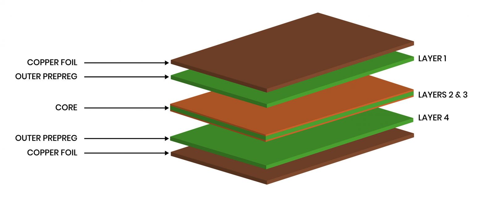
- Symmetry-First Principle: Multi-layer PCBs should maintain symmetrical copper distribution around the core layer. For example, a 4-layer board with a “2oz outer layer + 1oz inner layer” mirror structure prevents warping caused by mismatched thermal expansion coefficients. This symmetry applies not only to copper thickness but also to dielectric layer thickness matching.
- Dynamic Load Balancing: High-frequency signal layers should form tight coupling with adjacent ground planes to minimize electromagnetic interference (EMI) by shortening return paths. Power and ground layers require optimal spacing to prevent capacitive coupling failure while avoiding dielectric breakdown risks.
2. Three-Dimensional Thermal Management
- Integrated Heat Dissipation Networks: For high-heat sources like BGAs, adopt a “surface copper + thermal vias + backside copper block” composite structure. A 0.3mm-diameter thermal via array can reduce thermal resistance by 40%, replacing traditional heat sinks.
- Intelligent Copper Zone Planning: Implement “copper isolation zones” around power devices: Use ring-shaped copper barriers at power inputs for EMI shielding and chessboard-patterned copper division to balance local thermal density. This design reduces IGBT module operating temperatures by 15°C.
3. Copper Layer Synergy for Signal Integrity
- New Paradigm for Impedance Control: Differential pairs require “adjacent-layer effect” consideration: A 0.14mm dielectric thickness achieves 100Ω impedance when signal layers neighbor ground planes. If adjacent to power layers, increase thickness to 0.18mm to compensate for capacitive coupling.
- Electromagnetic Optimization of Vias: High-speed signal vias should use “anti-pad + back-drilling” techniques: A 0.2mm isolation zone around vias, combined with removing >10mil excess via wall copper, reduces signal attenuation by 3dB.
4. Manufacturing Compatibility Design
- Copper Thickness Gradient Management: Mixed copper thickness designs must follow “thick-to-thin” stacking: Place 3oz outer layers on the surface and 1oz inner layers beneath. This reduces side-etching during etching, maintaining line width tolerance within ±10%.
- Manufacturability Pre-Checks: Simulate copper deposition uniformity during design: Test pads at PCB edges detect plating current density distribution. If edge-to-center thickness difference exceeds 15%, adjust fixture design or switch to pulse plating.
5. Innovative Applications of Functional Copper Layers
- Embedded Passive Components: Embed copper inductors in high-frequency inner layers: Spiral copper patterns with magnetic dielectric layers achieve 10nH inductance in a 5mm×5mm area, replacing discrete components.
- Flexible Region Copper Treatment: Rigid-flex PCBs should use “meshed + solid” hybrid copper in flex areas: 0.05mm-wide copper meshes in bend zones transition to solid copper elsewhere, increasing flex life to 100,000 cycles.
6. Reliability Enhancement Designs
- Mechanical Stress Buffering: Implement “copper thickness gradient” designs near connectors: Reduce copper thickness from 3oz to 1oz within 0.5mm of pad edges to distribute mechanical stress, tripling insertion/removal lifespan.
- Corrosion Protection Systems: Coastal-environment PCBs require “dual-layer protection”: Deposit 1μm nickel followed by 2μm ENIG (electroless nickel immersion gold) to extend salt spray test survival from 48 to 200 hours.
7. Advanced Design Verification Methods
- Thermal-Mechanical Coupling Simulation: Use multi-physics tools to simulate copper distribution’s impact on board deformation. When copper coverage exceeds 60%, add 0.2mm prepreg as a stress buffer in critical zones.
- Signal-Power Co-Simulation: Optimize copper configurations via SI/PI joint analysis: Increasing DDR4 power layer copper from 1oz to 2oz reduces IR drop from 50mV to 20mV while maintaining >80% signal eye diagram opening.
PCB Copper Layer Failure Modes & Countermeasures
1. Copper Delamination
- Failure Mode: Separation between the copper layer and substrate due to thermal stress, mechanical impact, or chemical corrosion, commonly observed during high-voltage testing or thermal cycling of multilayer boards.
- Countermeasures: Optimize lamination process parameters (temperature gradient ≤5℃/min), select high-Tg substrates (Tg≥170℃), and enhance adhesive coating uniformity between copper foil and substrate.
2. Copper Corrosion
- Failure Mode: Copper surface oxidation or electrochemical corrosion triggered by moisture or contaminants (e.g., chloride ions, sulfides), leading to circuit breaks or impedance anomalies.
- Countermeasures: Apply surface finishes like ENIG (Electroless Nickel Immersion Gold) or OSP (Organic Solderability Preservative), strictly control ambient humidity (RH≤40%), and design drainage channels at PCB edges to reduce contaminant deposition.
3. Copper Over-Etching
- Failure Mode: Improper control of etching solution concentration, temperature, or duration, resulting in jagged copper line edges or line width deviations (>±15%), compromising signal integrity.
- Countermeasures: Establish etching process windows (e.g., maintain copper chloride solution temperature at 50±2℃), and adopt laser direct imaging (LDI) technology to replace traditional exposure for improved line width accuracy.
4. Copper Micro-Cracking
- Failure Mode: Fine cracks within the copper layer caused by bending or vibration stress, particularly prone to intermittent breaks in flexible PCBs (FPCs) or high-density interconnect (HDI) boards.
- Countermeasures: Use low-profile copper foil (HA type), align substrate rolling direction with stress application direction, and design buffer copper structures (e.g., mesh patterns) in flex regions.
5. Copper Electromigration
- Failure Mode: Copper ion migration along grain boundaries under high current density, forming dendritic shorts (especially when power layer-to-signal layer spacing <0.2mm), common in high-power PCBs.
- Countermeasures: Increase copper layer thickness (≥2oz), introduce barrier layers (e.g., Ni layers) to suppress ion migration, and optimize current distribution via simulation to reduce local hotspot temperatures.
Frequently Asked Questions
Q1: Why do high-speed PCBs require thinner copper layers for inner layers?
A1: Thinner copper layers (e.g., 0.5oz/17?m) are critical for high-speed PCBs operating at frequencies ≥5GHz, as they minimize dielectric loss and skin effect by reducing inductance and parasitic capacitance. Using thicker copper on inner layers can degrade signal integrity, so designers typically pair 0.5oz copper for inner layers with 1oz copper on outer layers, while selecting low-loss substrates like Rogers 4350B to optimize performance.
Q2: How to prevent copper imbalance in multilayer PCBs?
A2: Copper imbalance, which leads to board warping during thermal cycling, can be mitigated by evenly distributing copper across layers—aiming for 70% coverage per layer—and adding dummy copper fills in sparse regions to maintain symmetry. Designers should also use symmetric stack-ups, such as a 4-layer “Signal-Power-Ground-Signal” configuration, and leverage design software tools like Altium’s “Copper Pour” feature to verify balance before manufacturing.
Q3: What causes copper voids in via plating, and how to fix them?
A3: Copper voids in via plating typically result from trapped air bubbles, resin smear, or uneven electroplating conditions. To resolve this, designers should replace permanganate desmearing with plasma treatment for deeper vias, optimize plating parameters by reducing current density to 1.5–2A/dm? while increasing agitation, and avoid excessive via aspect ratios (>6:1 depth-to-diameter). Backdrilling stubs can further enhance reliability in high-speed designs.
Q4: Can copper layers be too thick for high-current PCBs?
A4: While thick copper (>3oz/105?m) improves current capacity, it complicates etching precision and drives up costs. Instead, designers should calculate optimal trace widths for current demands (e.g., 10mm width for 20A at 2oz copper), distribute current across multiple thinner layers in parallel (e.g., two 2oz layers), and incorporate thermal vias (0.3–0.5mm diameter, spaced 1mm apart) to enhance heat dissipation without relying solely on thicker copper.
Q5: Why does copper peel off after thermal cycling, and how to prevent it?
A5: Copper peeling after thermal cycling stems from inadequate adhesion between the copper layer and substrate, often caused by insufficient surface treatment or improper lamination. To prevent this, designers should apply black or brown oxide coatings before lamination to improve bonding, increase lamination pressure to 50–60kg/cm? for high-Tg materials (Tg≥170℃), and opt for surface finishes like ENIG (gold) instead of HASL, as ENIG provides superior adhesion and corrosion resistance in harsh environments.
Tags: PCB copper layer