

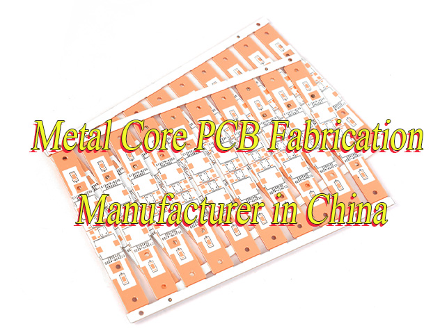
Looking for reliable metal core PCB fabrication manufacturer? Let’s explore its definition, types, production process, recommended MCPCB manufacturer.
Are you worried about these problems?
- Is long lead time for metal-core PCB delaying your project progress?
- Struggling with high-power heat dissipation, forcing repeated thermal layout adjustments?
- Balancing high material costs against performance needs in your budget?
As a MCPCB manufacturer, EBest Circuit (Best Technology) can provide service and solutions:
- 24-Hour Rapid Prototyping: Receive physical samples by next day, accelerating prototype validation without project delays.
- Customized Thermal Management: Leverage aluminum-based (≥2.0W/m·K) and copper-based (≥380W/m·K) high thermal conductivity, combined with thermal simulation, to maintain ≤20℃ temperature rise in high-power applications.
- Transparent Cost Control: No hidden fees, material costs reduced by 30%, with clear tiered pricing and bulk order discounts for precise budget planning.
Welcome to contact us if you have any request for metal core PCB fabrication: sales@bestpcbs.com.
What is Meant by Metal Core PCB Fabrication?
Metal Core PCB Fabrication refers to the process of manufacturing printed circuit boards using metal materials such as aluminum, copper, or steel alloys as the core heat dissipation layer through processes such as lamination, drilling, and surface treatment. Its core feature is the high thermal conductivity of the metal substrate to achieve efficient thermal management. It is widely used in scenarios that require rapid heat dissipation, such as LED lighting, power modules, automotive electronics, and high-power industrial equipment.
Types of Metal Core PCB Fabrication
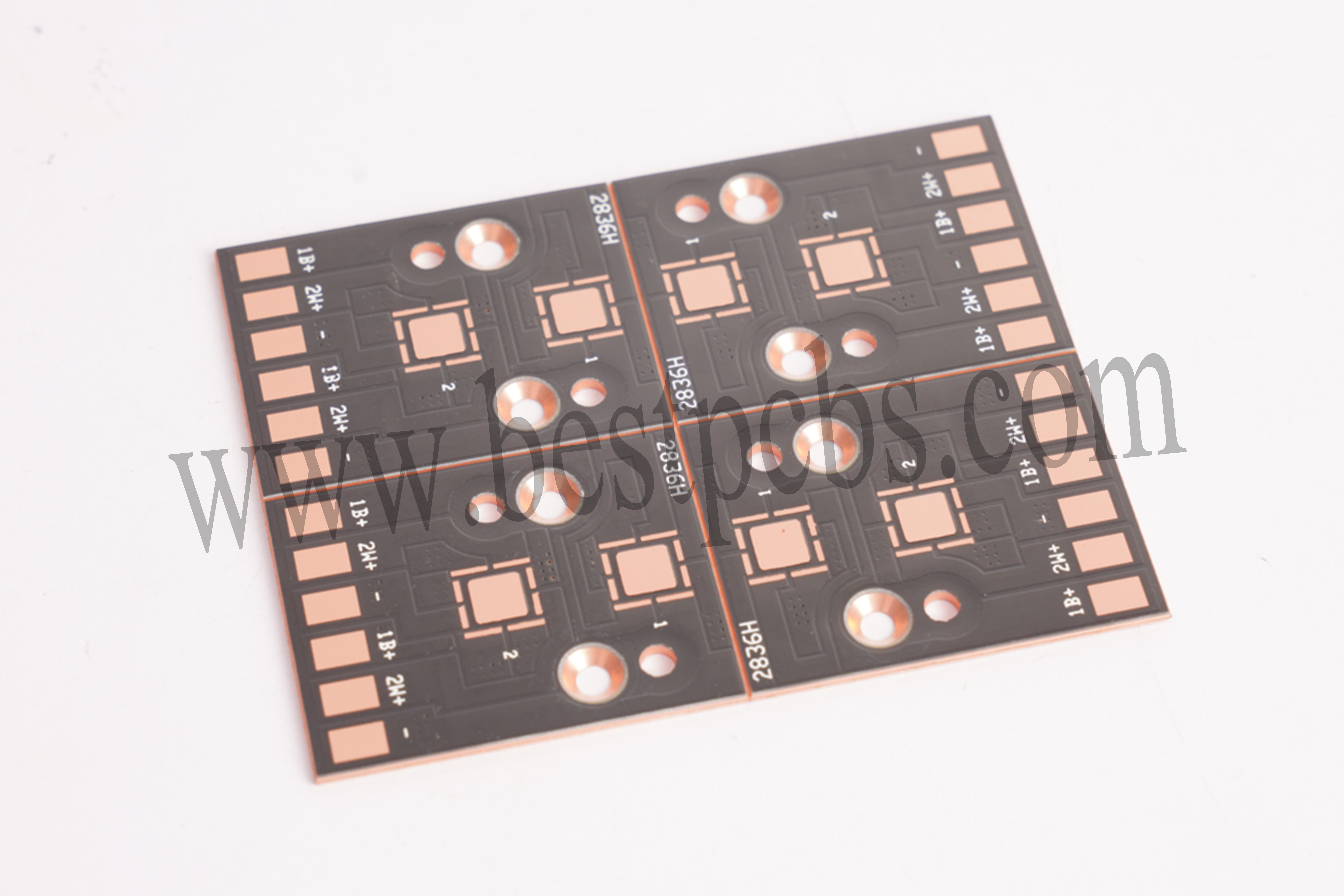
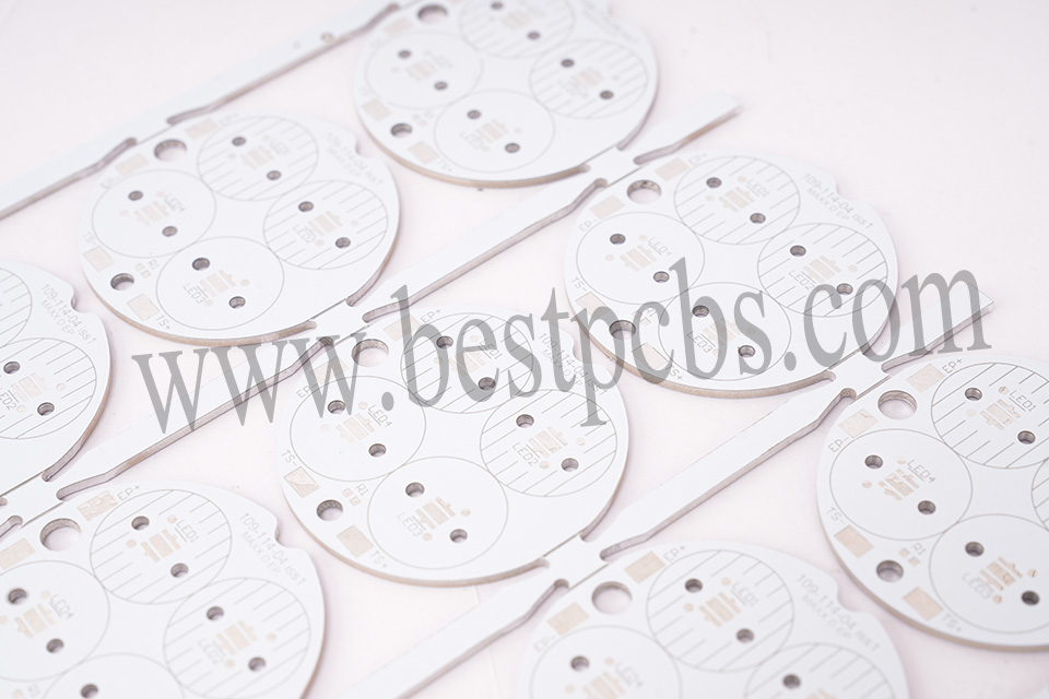
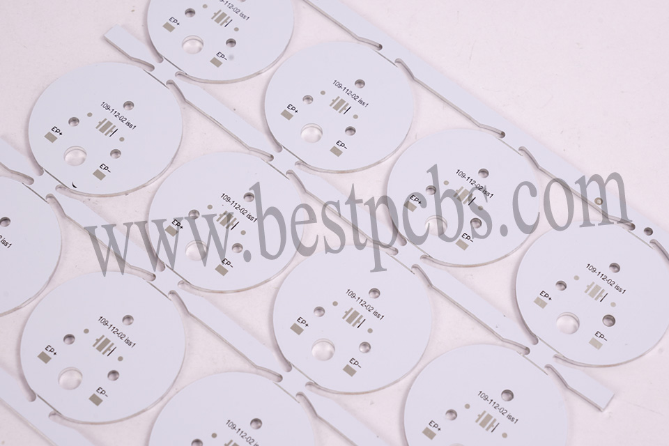
- Aluminum Core PCB: Using 5052/6061 aluminum alloy as the core material, it combines lightweight properties with high thermal conductivity (1-2W/mK or higher) and excellent cost-effectiveness. Widely applied in LED lighting, automotive electronics, and power modules, it supports single-layer to multi-layer structural designs to meet high-density integration and efficient heat dissipation requirements.
- Copper Core PCB: Employing pure copper or copper alloy substrates, it offers superior thermal conductivity (exceeding 4W/mK) and significantly better heat dissipation efficiency compared to aluminum-based materials, though at a higher cost. Ideal for high-frequency circuits, high-power laser devices, and medical imaging equipment where extreme heat dissipation is critical, often enhanced with surface plating (e.g., immersion gold, silver plating) for improved solderability.
- Iron-Core Metal PCB: Based on ordinary steel or stainless steel, it features high mechanical strength and better thermal conductivity than traditional FR-4 materials (though lower than aluminum/copper). Commonly used in precision scenarios requiring controlled thermal expansion coefficients, such as LED packaging, industrial power modules, and specific optical devices, balancing heat dissipation with structural stability.
- Hybrid-Pressure Metal Core PCB: Combining metal substrates (e.g., aluminum/copper) with FR-4 or other insulating materials to form a composite structure. It balances signal integrity and heat dissipation needs, suitable for complex electronic systems requiring both high-frequency signal transmission and efficient heat management, such as 5G base station RF modules and industrial controllers.
Aluminum Metal Core PCB Fabrication Processes
Below are aluminum metal core PCB fabrication processes:
1. Base Material Cutting and Pretreatment
- Material Selection: Utilize C1100 pure copper substrate with thermal conductivity ≥380W/(m·K), thickness tolerance ±0.02mm, and surface roughness Ra≤0.8μm.
- Precision Cutting: Cut to design dimensions (e.g., 100mm×100mm to 500mm×600mm) using CNC equipment, with edge chamfering to prevent burrs and dimensional accuracy ±0.05mm.
- Surface Enhancement: Ultrasonic cleaning removes oil contaminants; sandblasting or chemical etching (sulfuric acid-hydrogen peroxide system) increases bonding strength, with roughness controlled at 1.5-3.0μm.
2. Circuit Production Full Workflow
- Dry Film Application: Apply LDI-specific dry film (8-12μm thickness), use laser direct imaging (LDI) for high-precision transfer (line width/spacing ≥50μm), and set exposure energy at 100-150mJ/cm².
- Etching Process: Alkaline etching solution (copper chloride system) operates at 45-50℃ with an etching rate of 1.0-1.5μm/min; spray systems ensure uniform etching, and side etching is limited to ≤0.05mm.
- Quality Verification: Visual inspection checks for cracks/defects; AOI detects shorts/opens; in-circuit testing (flying probe) validates electrical continuity, targeting ≥99.5% yield.
3. Interlayer Dielectric Lamination and Drilling
- PP Lamination: High-Tg (≥170℃) semi-cured sheets (e.g., FR-4 epoxy) are heat-pressed (180-200℃, 3.0-4.0MPa) to eliminate bubbles and delamination.
- Precision Drilling: CNC or laser drilling achieves hole diameter accuracy ±0.05mm, wall roughness Ra≤3.2μm, and cleanliness meeting IPC-6012 standards.
4. Lamination Process Optimization
- High-Temperature High-Pressure Lamination: At 200-220℃ and 4.0-5.0MPa for 60-90 minutes, copper substrate and cover film fuse into a void-free integrated structure.
- Stripping Treatment: NaOH solution (5-10%) at 50-60℃ removes residual dry film within 3-5 minutes without damaging copper circuits; pure water rinse and drying follow.
5. Surface Treatment and Protection
- Solder Mask: Liquid photosensitive ink (20-30μm) is UV-cured to form a durable protective layer (temperature resistance ≥300℃, insulation ≥10¹²Ω) with precise patterning via development.
- Character Printing: Screen-printed white/black ink cures at 150℃ for 60 minutes, ensuring smudge-free legibility and alcohol resistance ≥50 cycles.
Surface Finishes:
- OSP: 0.2-0.5μm organic coating, lead-free and eco-friendly, ideal for short-term storage.
- Immersion Gold: Au 0.05-0.1μm/Ni 3-5μm, excellent corrosion resistance for high-frequency applications.
- Lead-Free HASL: 5-8μm Sn-Ag-Cu alloy, RoHS-compliant with robust solder joint reliability.
6. Profile Processing and Dimensional Control
- Cutting Precision: CNC routing or laser cutting maintains ±0.1mm accuracy; V-CUT depth is controlled at 1/3-2/3 of board thickness, with burr-free edges.
- Performance Testing: Continuity checks, insulation resistance (≥500MΩ), voltage withstand (AC 1000V/minute), and thermal imaging verify heat dissipation uniformity (temperature rise ≤20℃).
7. Full-Process Quality & Environmental Management
- Process Control: SPC monitoring with CPK≥1.33; real-time parameter tracking and automatic alarms at each inspection point.
- Eco-Compliance: Waste etching solution is neutralized/precipitated for licensed disposal; waste gas undergoes activated carbon adsorption + catalytic combustion to meet ISO 14001 standards.
- Traceable Packaging: Vacuum-sealed packaging with anti-moisture/oxidation protection; each batch includes QC reports, MSDS, RoHS certificates, and QR code traceability for full production data.
Our Custom Metal Core PCB Fabrication Options
Below are custom options for metal core PCB fabrication:
- Substrate Metal Type Customization: Selectable aluminum-based, copper-based, iron-based, or composite metal alloy substrates, with thickness customization available from 0.5mm to 5mm, balancing thermal conductivity and cost efficiency.
- Layer Count & Structural Configuration: Supports single-layer to 8-layer+ metal-core PCB structures, with flexible signal/power/ground layer distribution to accommodate high-density integration, high-frequency signal transmission, or high-power circuit requirements.
- Thermal Management Specialized Design: Integrates thermal via arrays, thermal interface material (TIM) coatings, or finned heat sink topologies, leveraging high thermal conductivity of metal substrates for precise chip-to-system thermal path optimization.
- Surface Finish Options: Offers surface treatments including ENIG (Electroless Nickel Immersion Gold), OSP (Organic Solderability Preservative), HASL (Hot Air Solder Leveling), and chemical nickel-gold, ensuring soldering reliability, oxidation resistance, and long-term stability.
- Precision Line & Via Parameters: Supports 20μm minimum line width/spacing precision etching, with mechanical/laser drilling and blind/buried via capabilities for 0.1mm-1.0mm via diameters, meeting high-density interconnect demands.
- Custom Shape & Contour Machining: Enables non-standard dimensions (e.g., circular, annular, polygonal) and complex contour cutting, including V-cut scoring, milling slots, and chamfering for device structural fit and assembly requirements.
- Solder Mask & Identification Customization: Multi-color solder mask options (green, black, white, etc.), with customer-specified logo, model identification, and QR code etching for traceability and brand recognition.
Why Choose EBest Circuit (Best Technology) as Metal Core PCB Fabrication Manufacturer?
Reasons why choose us as metal core PCB fabrication manufacturer:
- 19-Year Metal-Core PCB Manufacturing Expertise: Leverage mature process libraries for rapid implementation of single-layer to multi-layer metal-core substrates (aluminum/copper/iron-based), reducing trial-and-error costs by over 30% through parameterized design templates.
- Dual Medical & Automotive Certifications: ISO 13485 (medical) and IATF 16949 (automotive) quality certifications ensure direct compliance for projects in these sectors, shortening product launch cycles by 2-4 weeks.
- 24-Hour Rapid Prototyping: Same-day design-validation closure and next-day physical prototype delivery for urgent projects, accelerating prototype iteration and market entry.
- Full-Process 12-Step SPC Quality Control: Batch-specific CPK≥1.33 test reports for thickness, thermal conductivity, and insulation resistance, ensuring ≥99.5% yield and minimizing rework losses.
- Transparent Tiered Pricing with No Hidden Costs: Avoid expenses such as mold fees and engineering fees; bulk orders enjoy 30% cost optimization for metal-core materials, with clear budgeting support.
- One-Stop Metal-Core PCB Full-Process Service: Covers design support, prototyping, mass production, surface treatment (ENIG/OSP), and assembly testing, eliminating multi-supplier coordination and saving 50% communication costs.
- Free Metal-Core DFM Design Optimization: Identify process risks (e.g., thermal stress, circuit etching defects) to optimize layout and material selection, reducing production costs by over 20% and enhancing manufacturability.
- Customized Metal-Core Thermal Management Solutions: Leverage high thermal conductivity (aluminum ≥2.0W/m·K, copper ≥380W/m·K) for thermal via design, heat sink integration, and thermal simulation, ensuring ≤20℃ temperature rise in high-power scenarios.
How to Get a Quote for Metal Core PCB Fabrication Service?
Below is material list for MCPCB quotation:
Substrate Type and Specifications
- Specify the type of metal substrate (aluminum-based/copper-based/iron-based) and specific models (e.g., aluminum-based 5052, copper-based C1100). Include thermal conductivity requirements (e.g., aluminum-based ≥2.0W/m·K, copper-based ≥380W/m·K).
- Provide substrate thickness range (e.g., 0.8-3.2mm) and copper foil thickness (1-8 ounces), with tolerance requirements (±0.02mm).
Circuit Layer Design Parameters
- Submit Gerber files or PCB design drawings, including line width/spacing (e.g., ≥50μm), minimum aperture (e.g., 0.3mm via/0.1mm blind via), and special wiring requirements (e.g., high-frequency signal isolation).
- Specify the layer structure (single-layer/double-layer/multi-layer) and interlayer connection methods (through-hole/blind via/buried via).
Surface Treatment and Protection Requirements
- Select surface treatment processes: OSP, immersion gold (Au 0.05-0.1μm/Ni 3-5μm), lead-free HASL (tin-silver-copper alloy), or electroplated nickel-gold, with specific thickness and environmental standards (e.g., RoHS).
- Solder mask color (green/black) and silk screen requirements (white/black characters), with specified alcohol resistance (≥50 cycles).
Special Process and Certification Requirements
- Specify whether medical-grade ISO 13485 or automotive-grade IATF 16949 certification is required, along with environmental standards (e.g., ISO 14001).
- Specify special process requirements: laser drilling, CNC forming, V-CUT scoring, or assembly testing (e.g., flying probe test/AOI inspection).
Batch Quantity and Delivery Requirements
- Provide order quantity (e.g., 5-10 prototype pieces/1000+ batch pieces) and delivery time requirements (e.g., 24-hour rapid prototyping/regular 7-10 days).
- Specify packaging requirements (vacuum packaging/moisture-proof bags) and logistics methods (air/sea freight).
Welcome to contact us if you have any request for metal core PCB fabrication service: sales@bestpcbs.com.