

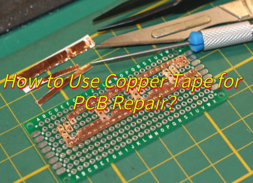
How to use copper tape for PCB repair? Let’s explore benefits, applications, usage process, tools and material list, copper tape types, testing methods, and maintenance tips for copper tape PCB repair.
As a professional PCB manufacturer, EBest Circuit (Best Technology) can provide you PCB repair service:
- Free Technical Support: Provide evaluation of repair alternatives.
- Repair multilayer boards: Supports blind and buried hole conductivity.
- 24 Hours Rapid Prototyping: Quickly replace the broken PCB board.
Welcome to contact us if you have any request for PCB repair or PCB prototyping: sales@bestpcbs.com.
Why Choose Copper Tape for PCB Repair?
Reasons why choose copper tape for PCB repair:
Fast Repairs, Save Time
- No need for complex tools or long waits, just cut and stick the copper tape, then solder. Perfect for fixing broken traces or lifted pads quickly.
- Great for emergencies or prototyping, reducing equipment downtime.
Excellent Conductivity, Stable Signals
- Pure copper with conductive adhesive ensures low resistance (usually ≤50mΩ), matching original circuit performance.
- Avoids signal issues caused by poor connections.
Flexible and Easy to Use
- Bend and cut copper tape to fit tight spaces or complex PCB layouts (e.g., keyboard circuits, sensors).
- Less risk of short circuits compared to jumper wires.
Low Cost, High Value
- Much cheaper than custom PCBs or professional repair services. Ideal for small batches or hobbyists.
- One roll lasts for multiple repairs, offering long-term savings.
Versatile Applications
- EMI Shielding: Reduces electromagnetic interference.
- Quick Prototyping: Test circuit designs without remanufacturing PCBs.
- Grounding: Provides reliable ground connections for components.
Works with Most PCB Materials
- Suitable for FR-4, CEM-1, and other common substrates, as well as gold-plated or ENIG finishes.
- Strong adhesive holds up under high temperatures (compatible with reflow soldering).
Applications of Copper Tape PCB Repair
- Fix Broken Traces: Layer copper tape over cut or damaged traces and solder ends.
- Replace Lifted Pads: Stick copper tape where pads detached; solder components to it.
- Bridge Missing Connections: Use tape to jump gaps where traces are missing.
- Reinforce High-Stress Areas: Add tape to flexed PCB zones (e.g., connectors) to prevent breaks.
- Quick Prototyping: Temporarily modify or add circuits without etching new PCBs.
- EMI Shielding: Cover sensitive parts with tape to block interference.
- Ground Components: Create low-resistance ground paths for noise reduction.
- Repair Keyboard Membranes: Patch broken conductive traces on flexible keyboard circuits.
How to Use Copper Tape for PCB Repair?
Below are steps of copper tape for PCB repair:
1. Inspect and Clean the Damaged Area
- Visually locate the broken trace. Use a magnifier to confirm the damage range.
- Clean the area with an alcohol-soaked cotton swab to remove residue, oxidation, or solder mask. If the solder mask covers the break, scrape it off with a blade or sandpaper to expose the copper base.
2. Cut the Copper Tape
- Trim the tape to match the broken trace’s shape, ensuring it’s slightly larger than the damaged zone (covering intact copper on both ends).
- The tape width should match the original trace. Length must span the break and overlap adjacent copper (at least 1-2mm).
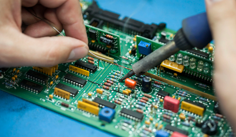
3. Apply the Copper Tape
- Press the tape flat onto the break, ensuring full contact with exposed copper and no air bubbles.
- The tape must fully cover the break and extend to nearby pads or vias for reliability.
4. Solder to Secure
- Quickly solder the tape’s ends to the PCB copper. Avoid overheating (back adhesive may melt).
- Use low-temperature solder. Keep the iron’s contact time under 2 seconds to prevent tape detachment.
- If repairing a pad, solder the component lead to the tape simultaneously.
5. Trim Excess Tape
- Carefully cut or scrape the tape edges to match the original trace width.
- Warning: The repair is fragile—avoid excessive force to prevent lifting.
6. Reinforce and Insulate
- (Optional) Cover the tape with insulating tape (e.g., Kapton) or apply solder mask to prevent shorts or damage.
- For high-stress areas (e.g., PCB edges), reinforce with epoxy (e.g., Araldite).
7. Test Functionality
- Use a multimeter to check continuity (resistance should be near 0Ω).
- Power on the device and monitor for poor contact or overheating.
Copper Tape for PCB Repair Tools & Material List
| Tool/Material | Purpose |
| Single-Sided Conductive Copper Foil Tape | Bridge broken traces, repair pads, restore copper foil. |
| Isopropyl Alcohol (IPA) + Swabs | Clean oxidation, flux residue, or solder mask from repair area. |
| Fiber Pen/Engraving Knife | Mark repair zone or scrape solder mask covering breaks. |
| Soldering Iron (250–300°C) | Solder copper tape to PCB traces for low-resistance contact. |
| Lead-Free Solder Wire | Reinforce joints to reduce contact resistance. |
| Hot Air Gun (80–100°C) | Soften adhesive for better tape adhesion (optional). |
| Scissors/Precision Knife | Trim tape edges to match trace width; prevent field concentration. |
| 600-Grit Sandpaper | Lightly abrade copper for improved adhesion (oxidized areas only). |
| Conformal Coating/UV Mask | Insulate and protect repair from oxidation/shorts. |
| Kapton Tape | Secondary insulation for tape edges; high-temp resistant. |
| Epoxy Resin (e.g., Araldite) | Reinforce high-stress areas (edges, connectors). |
| Multimeter (Resistance Mode) | Verify continuity (resistance ≈ 0Ω); check for abnormal heating post-repair. |
Types of Copper Tape Suitable for PCB Repair
1. Single-Sided Conductive Copper Foil Tape
- Use: Fix broken traces, repair missing pads, fill copper foil defects.
- Application: General PCB repairs, such as signal line breaks or component pin detachment.
2. Double-Sided Conductive Copper Foil Tape
- Use: Cross-layer conductive connections (e.g., shielding repairs), multilayer board grounding.
- Application: requiring bidirectional conductivity, like high-frequency circuit shielding or shorting between layers.
3. High-Temperature Copper Foil Tape
- Use: Repairs in high-temperature environments (e.g., power modules, LED driver boards).
- Application: Fixing lines near heat-generating components or temporary patching for reflow soldering.
4. Ultra-Thin Copper Foil Tape (≤10μm)
- Use: High-density PCB repairs (e.g., BGA pad rework, fine-pitch traces).
- Application: Precision fixes in tight spaces to avoid interference with component installation.
5. Corrosion-Resistant Zinc-Plated Copper Foil Tape
- Use: Repairs in humid or corrosive environments (e.g., outdoor equipment, industrial control boards).
- Application: Extend repair lifespan in salt-fog or moisture-heavy conditions.
6. Non-Conductive Adhesive Copper Foil Tape
- Use: High-voltage circuit repairs (e.g., power board isolation), insulating layer patches.
- Application: Where adhesive must not create electrical contact to prevent shorts.
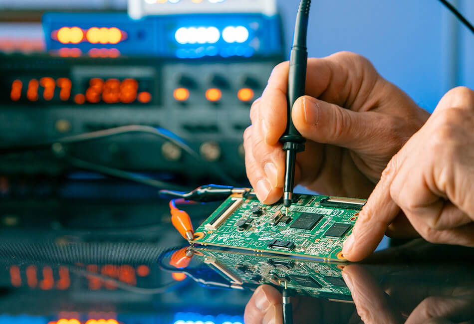
Testing and Verifying Repaired PCB Functionality
1. Visual Check
- Look for visible flaws on the repaired PCB, like solder bridges, cold joints, or damaged parts.
- Confirm components are placed and oriented correctly as per the design.
2. Continuity Test
- Use a multimeter to check electrical continuity between key points, e.g., power/ground traces and component connections.
- Ensure no open or short circuits exist.
3. Power-Up Test
- Connect PCB to power supply and slowly raise voltage to operating level.
- Watch power consumption; check for abnormal current or voltage issues.
4. Function Test
- Create and run a full test plan covering all PCB functions.
- Use tools like logic analyzers or oscilloscopes to verify digital and analog circuit operation.
- Test under different conditions (voltages, frequencies, loads) for stability.
5. Signal Test
- For high-speed or sensitive signals, check for crosstalk, reflections, and jitter.
- Use TDR or similar methods to analyze signal quality.
6. Thermal Test
- Monitor PCB and component temperatures during operation; ensure they’re within limits.
- Use thermal cameras or sensors to find hot spots or excessive heat.
7. Environment Test
- Put PCB through stress tests like temperature cycling, humidity, and vibration.
- Confirm it still works after each test with no degradation.
Long-Term Maintenance Tips for Copper Tape Repairs
1. Keep It Clean
- Wipe the repair area with a dry cloth to remove dust.
- Use isopropyl alcohol (90%+) and a cotton swab for spills, avoid scrubbing.
2. Block Moisture
- Coat the copper tape with non-conductive epoxy or conformal coating.
- Store/operate PCBs in a dry place (<60% humidity).
3. Avoid Bending/Pressure
- Don’t flex or twist flexible PCBs near the repair.
- Keep heavy objects off the repaired area.
4. Check for Corrosion
- Inspect every 3–6 months for discoloration or lifting edges.
- Test with a multimeter for unexpected resistance.
5. Strengthen High-Use Joints
- Add solder to frequent connections for durability.
- Secure tape edges with non-conductive glue/epoxy.
6. Avoid Extreme Temps
- Keep repairs away from heat sources (e.g., motors).
- Prevent rapid cold exposure to avoid condensation.
7. Track Repairs
- Label the repair site (e.g., “R12 – Copper Fix”).
- Log dates/issues in a maintenance notebook.
8. Replace if Needed
- If the tape cracks, corrodes, or peels, remove and reapply a new piece.
FAQs of Copper Tape for PCB Repair
Q1: Why does copper tape for PCB repair peel off?
A1: Clean the PCB with alcohol and a cloth. Use strong-adhesive copper tape and press firmly with a flat tool.
Q2: Why do copper tape connections cut in and out?
A2: Press out air bubbles with a smooth tool. Add solder to key spots after sticking the tape for better contact.
Q3: Why does copper tape cause shorts or breaks?
A3: Line up the tape carefully using a magnifier. Hold it in place with masking tape before pressing down.
Q4: Why does copper tape corrode or dull?
A4: Coat the repair with epoxy or conformal coating to block moisture. Store extra tape in a dry, sealed spot.
Q5: Why are solder joints on copper tape weak?
A5: Use low heat when soldering and avoid overheating. Clean off flux residue with alcohol after soldering.