

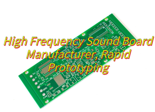
How to design high frequency board? This guide covers material selection, 6GHz design rules, frequency stability control, and cost-saving strategies for high-performance PCBs.
Are you troubled with these problems?
- Why do high-frequency signals distort at critical bands?
- Why do promised substrate parameters consistently fail real-world testing?
- Why are costs for low-volume high-frequency PCBs prohibitively high?
As a high frequency PCB manufacturer, EBest Circuit (Best Technology) can provide you service and solution:
- Precision Impedance Control – Signal loss <0.5dB/inch for frequencies ≤24GHz.
- Verified Real-World Data – Batch-specific Dk/Df test reports included.
- Cost-Optimized Manufacturing – Hybrid material design cuts costs by 30%.
Welcome to contact us if you have any request for high frequency board: sales@bestpcbs.com.
What Is High Frequency Board?
High Frequency Boards are printed circuit boards (PCBs) specifically designed for high-frequency signal transmission. They utilize special materials with low dielectric constant (Dk) and low dielectric loss (Df), such as PTFE and ceramic-filled composite materials, to ensure high stability and low attenuation during signal transmission. These boards are applied in fields with stringent requirements for signal integrity, including 5G communication, radar systems, satellite equipment, and high-speed digital circuits. Through precise design and surface treatment processes, they minimize signal distortion and electromagnetic interference.
How to Choose Materials for High Frequency Board Design?
1. Prioritize Electrical Performance Parameters
- Dielectric Constant (Dk): Select materials with low Dk (ideal range 3-3.5) to reduce signal delay and phase distortion. For high-frequency applications (e.g., millimeter wave), pursue the lowest Dk possible as losses increase with frequency.
- Loss Factor (Df/tanδ): Lower Df values minimize signal attenuation. FR-4 exhibits significant loss in GHz bands; high-frequency scenarios require materials with Df < 0.005 (e.g., PTFE).
2. Frequency Range Determines Material Type
- <5GHz: Modified FR-4 balances cost and performance, suitable for consumer electronics.
- 5-10GHz: Use ceramic-filled PTFE or polyimide for medium-high performance.
- 10GHz/Millimeter Wave: Ultra-low-loss materials (e.g., pure PTFE, Rogers series) are mandatory; traditional FR-4 fails completely.
3. Thermal-Mechanical Performance Matching
- Coefficient of Thermal Expansion (CTE): Must align with copper foil to prevent delamination. High-frequency materials typically require CTE < 70ppm/°C. Temperature Resistance: High-power scenarios demand high thermal conductivity (>0.5W/mK) to avoid overheating.
- Moisture Absorption: Prefer materials with <0.1% absorption rate, as humidity changes affect Dk stability.
4. Manufacturability and Cost Balance
- Processing Difficulty: PTFE requires laser drilling and specialized surface treatments, costing 3-5 times more than FR-4. Hybrid stack-ups (critical layers: PTFE + standard layers: FR-4) optimize costs.
- Copper Foil Treatment: Use ultra-low-roughness copper (RTF/VLP types) to reduce skin-effect losses.
- Peel Strength: PTFE substrates have lower copper adhesion; assembly reliability must be evaluated.
5. Supplementary Considerations for Special Scenarios
- Impedance Control: Material thickness tolerance must be <10% to ensure impedance matching accuracy.
- Size Effects: Compact circuits may use high-Dk thin materials to mitigate wavelength compression impacts.
- Signal Integrity: Avoid splitting reference planes; provide clear return paths.
6 Ghz High Frequency Board Design Guidelines
1. Stack-Up & Routing
Multilaminate Design(Minimum 6-layer stack-up recommended)
- Top: Critical high-speed signals.
- Layer 2: Solid GND plane.
- Layer 3: High-speed differential pairs.
- Layer 4: VCC plane.
- Layer 5: Auxiliary GND plane.
- Bottom: General signals.
2. Routing Rules
- Avoid parallel routing in adjacent layers to prevent capacitive coupling.
- Use 45° bends/arcs for signal traces to minimize EMI.
- High-speed signal length tolerance: ±5mil; differential pair length mismatch <2mil.
- Impedance Control: Calculate characteristic impedance using tools (e.g., Polar SI9000). Target ±5% accuracy for 50Ω single-ended/100Ω differential traces.
3. Power & Grounding Design
Power Network
- Place power/ground planes adjacent to reduce loop inductance.
- Deploy 0.1μF + 10μF decoupling capacitor pairs near high-speed ICs (<2mm distance).
Grounding Strategy
- Maintain unbroken ground planes; avoid splits.
- Follow 20H rule: Shrink power plane edges inward by 20× stack-up spacing relative to ground.
- Use multipoint grounding to minimize ground bounce.
4. Component Placement
- Functional Zoning: Segregate RF/digital/power modules; position sensitive components (e.g., LCDs) away from high-speed ICs.
- Pin Optimization: Limit high-speed device pin routing bends to ≤1; avoid traces between pins to reduce parasitic capacitance.
- Thermal Management: Place high-power components near board edges; reserve ≥4oz copper foil for heat dissipation.
5. Signal Integrity Measures
- Transmission Line Design.
- Employ coplanar waveguide (CPW) structures for critical paths.
- Avoid crossing plane splits; add stitching capacitors if necessary.
6. Crosstalk Mitigation
- Maintain ≥3× line width spacing between adjacent signal traces.
- Shield clock signals with guard traces and ground stitching.
7. Manufacturing Requirements
- Microvia Technology: Utilize laser drilling (≤0.1mm aperture) and via-filling plating for HDI interconnections.
- Surface Finish: Apply ENEPIG or immersion silver for high-frequency conductivity.
- Soldermask Control: Limit LPI soldermask thickness to ≤15μm; maintain ±25μm window accuracy.
8. Verification & Testing
Pre-Simulation:
- Perform 3D EM simulation (HFSS/SIwave) to analyze S-parameters and EMI.
Prototype Validation:
- Verify impedance via flying probe testing.
- Validate signal rise time (<35ps) through TDR measurements.
9. Documentation
- Annotate high-speed constraints (length/impedance/topology) in schematics.
- Conflict Resolution Note: To address adjacent signal layers in 6-layer designs, implement orthogonal routing (perpendicular traces) and ensure interlayer dielectric thickness ≥8mil to reduce coupling.
How to Control Frequency Stability in High Frequency Board Design?
1. Material Selection for Low Temperature Drift
- Choose substrates with low TCDk (Temperature Coefficient of Dielectric Constant), ideally ≤20 ppm/°C (e.g., ceramic-filled PTFE or Rogers RO4000 series).
- Avoid materials with high moisture absorption (e.g., standard FR-4) to prevent Dk shifts due to humidity changes.
2. Precision Impedance Control
- Maintain ±5% impedance tolerance for critical traces (e.g., 50Ω single-ended, 100Ω differential) using stack-up simulations (e.g., Polar SI9000).
- Use coplanar waveguide structures with ground shielding to minimize crosstalk-induced impedance variations.
3. Thermal Management Design
- Via arrays and thermal copper pours: Connect high-power components to heat sinks or inner-layer ground planes to reduce thermal gradients.
- Thermal interface materials (TIMs): Improve heat dissipation from ICs to prevent frequency shifts caused by localized heating.
4. Stable Reference Clock Design
- Use low-phase-noise crystal oscillators (e.g., TCXO or OCXO) with frequency stability ≤±1 ppm over temperature.
- Shield clock traces with grounded guard traces and minimize trace length to reduce EMI-induced jitter.
5. Mechanical Stress Mitigation
- Controlled CTE (Coefficient of Thermal Expansion): Match substrate and copper foil CTE (<70 ppm/°C) to prevent warping or delamination under thermal cycling.
- Rigid-flex design: For dynamic applications, use flexible PCB sections to absorb mechanical stress without affecting high-frequency traces.
6. Environmental Shielding
- Conformal coating: Apply acrylic or silicone coatings to protect against moisture, dust, and corrosion.
- EMI gaskets: Seal enclosures with conductive gaskets to block external interference affecting frequency stability.
7. Validation & Testing
- Thermal cycling tests: Verify frequency stability (-55°C to 125°C) per IPC-TM-650 standards.
- S-parameter testing: Ensure insertion loss (IL) remains ≤0.5 dB/100 mm at target frequencies (e.g., 24 GHz).
What Cost-Reduction Strategies Work for High Frequency Board Production?
1. Design Optimization for Cost Reduction
- Layer Optimization: For high-frequency circuits (>100MHz), determine the optimal layer count through simulation to avoid over-design. For example, a 4-layer board reduces noise compared to a 2-layer board, but increased layers significantly raise costs.
- Path Simplification: Use short, straight traces to minimize vias and sharp turns, reducing signal loss and manufacturing costs. Maintain 100Ω impedance for differential signals and 50Ω for single-ended signals.
- Via Optimization: Reduce via count in RF paths to prevent ground plane fractures; employ backdrilling technology to remove excess via stubs, lowering signal reflection (note potential quality risks).
2. Material Selection Strategies
- Substrate Grading: Use low-cost FR4 for general areas and premium materials (e.g., Rogers) for RF/high-frequency zones. Adopt localized hybrid pressing to balance low-loss requirements and cost.
- Copper Foil Optimization: Select low-roughness copper foil to reduce skin-effect losses, or evaluate lower-grade materials meeting electrical specs to cut costs.
3. Production Process Optimization
- Panel Utilization Improvement: Optimize panel layouts (e.g., 12″×18″ panels with 10 boards) to reduce per-board costs by up to 20%.
- Process Simplification: Use Tenting methods to skip metal resist steps, shortening cycles and saving costs. Refine lamination parameters and alignment techniques to resolve hybrid-press warping/misalignment issues.
- Scalable Production: Bulk orders lower unit and logistics costs; scaling production (e.g., GW-level capacity) dilutes fixed costs.
4. Manufacturing & Supply Chain Management
- DFM (Design for Manufacturing): Incorporate assembly efficiency during design to minimize rework. Single-sided component placement simplifies soldering.
- Process Stability: Adopt high-precision solder paste printing to optimize filling, release, and cleaning, ensuring yield with lower material costs. Implement systematic controls (e.g., ISO certification) to enhance yield and reduce replenishment costs.
5. Technological Innovation & Validation
- Simulation-Driven Design: Leverage power integrity analysis and signal integrity simulations to optimize layouts and reduce trial-and-error costs.
- Embedded Components: Integrate passive components to shorten signal paths, lowering resistance losses and noise, achieving long-term cost savings.
- Advanced Packaging: Utilize high-integration ICs to reduce peripheral components, lowering assembly and board size costs.
Why Choose EBest Circuit (Best Technology) as High Frequency Board Manufacturer?
Reasons why choose us as high frequency board manufacturer:
- Fastest Turnaround – Industry-leading production cycles (prototypes in 24-48 hours, volume orders in 5-10 days)
- Reliable Quality – Certified IPC-A-610 Class 3 standards with 99.98% first-pass yield rate
- Competitive Pricing – Cost-optimized solutions without compromising quality (15-30% savings vs. industry averages)
- Stable Supply Chain – Long-term partnerships with component manufacturers ensuring material availability
- Precision Manufacturing for Signal Integrity: ±0.025mm drilling accuracy & ±1% impedance control solve 5G/mm Wave signal integrity challenges, validated by 67GHz testing to ensure lossless transmission, directly boosting product communication quality and market competitiveness.
- End-to-End Material Optimization: A portfolio of 50+ qualified laminates (including ultra-low-loss Rogers/Duroid) with strict tan δ (<0.0015) control delivers one-stop RF performance solutions from material selection to validation, reducing R&D trial costs.
- Integrated Thermal Management: Metal-core boards + embedded heat pipes (15W/cm² dissipation) prevent warping/delamination in high-power applications, enhancing device reliability and lifespan.
- Rapid Prototyping with DFM Feedback: 24-hour prototype turnaround + 4-hour DFM feedback accelerates development cycles, enabling faster time-to-market and market leadership.
- Multi-Layer Impedance Matching: Precise control of 50Ω single-ended/100Ω differential impedance with 3D simulation validation meets diverse high-frequency application needs.
- Cost-Efficient Panel Optimization: Intelligent panel layout (e.g., 12″×18″ multi-board arrays) improves material utilization, combined with scalable production to lower per-unit costs while maintaining quality.
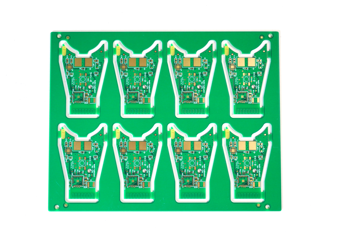
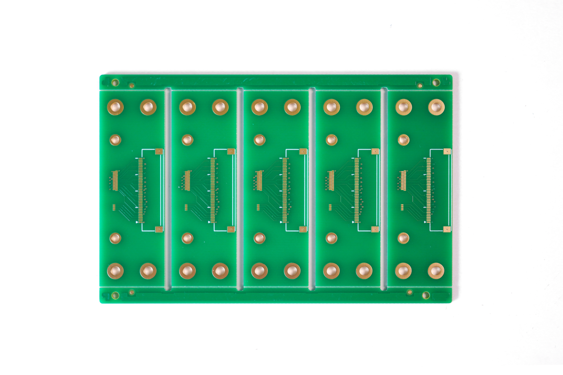
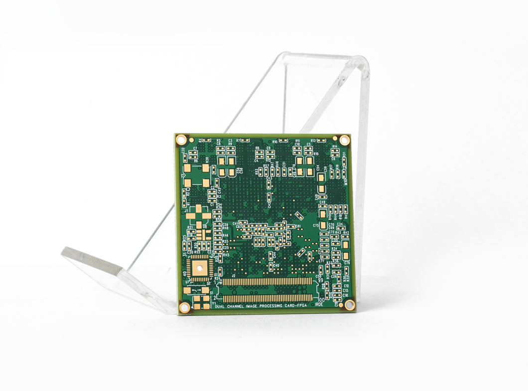
Below is a photo of high frequency PCB board we made before:
Our High Frequency Circuit Board Capabilities
| Base material: | Rogers/Telfon |
| Board Thickness: | 0.5mm~3.0mm(0.02″~0.12″) |
| Copper thickness: | 0.5 OZ, 1.0 OZ, 2.0 OZ, 3.0 OZ |
| Outline: | Routing, punching, V-Cut |
| Soldermask: | White/Black/Blue/Green/Red Oil |
| Legend/Silkscreen Color: | Black/White |
| Surface finishing: | Immersion Gold, HASL, OSP |
| Max Panel size: | 600*500mm(23.62″*19.68″) |
| Packing: | Vacuum/Plastic bag |
| Samples L/T: | 7~9 Days |
| MP L/T: | 8~10 Days |
How to Get a Quote for High Frequency Board Project?
1. Design Files
- Gerber files (all layers).
- Drill files (Excellon format).
- BOM (Bill of Materials) with part numbers/specifications.
2. Technical Specifications
- Substrate type (e.g., Rogers RO4350B, PTFE, ceramic-filled)
- Target Dk (2.0–3.5) and Df (<0.005) values
- Impedance requirements (e.g., 50Ω single-ended, 100Ω differential ±5%)
3. Layer Stack-Up
- Number of layers and copper weights (e.g., 2H/2L with 1oz inner, 2oz outer).
- Core/prepreg material and thickness per layer.
4. Surface Finish & Mask
- Finish type (ENEPIG, Immersion Silver, HASL, etc.).
- Solder mask color (LPI, thickness ≤15μm).
5. Mechanical Requirements
- Board dimensions and tolerances.
- Minimum trace/space widths (e.g., 3/3 mil).
- Via types (blind/buried/microvias, via-in-pad).
6. Testing & Quality
- Required tests: S-parameter, TDR, thermal cycling, X-ray for via fill.
- Acceptance criteria (e.g., IL ≤0.5 dB/100mm at 6 GHz).
7. Quantity & Lead Time
- Prototype vs. production volume (e.g., 10 pcs vs. 1,000 pcs).
- Target delivery timeline.
8. Special Requests
- Controlled impedance simulation reports
- Certifications (e.g., IPC-6012 Class 3, RoHS)
Welcome to contact us if you have any request for high-frequency board: sales@bestpcbs.com.
Tags: High Frequency Board