

Embedded copper technology is a specialized PCB manufacturing process that enhances current handling and thermal performance by embedding copper directly into the board’s layers. In the realm of printed circuit board (PCB) manufacturing, efficient heat dissipation is a critical factor, especially as electronic devices become more compact and powerful. One innovative solution that addresses this challenge is embedded copper technology. This process involves embedding copper blocks in specific areas of the board, allowing direct thermal transfer from heat-generating components to the copper, thereby achieving rapid heat dissipation. Let’s delve into the details of this technology, including its types, key parameters, and material requirements.
EBest Circuit (Best Technology) is a major PCB manufacturer in China, providing Embedded Copper PCB, embedded copper coin PCB, heavy copper PCB, and extra thin PCB in a rapidly expanding market. Our factory invites sophisticated embedded copper technology, embedded copper coin technology, and cutting-edge equipment for high-precision PCB manufacturing, enabling optimized thermal management and signal integrity solutions in 5G, EV, and aerospace applications. If you would like to enquire about the embedded copper technology price or need any technical support, just feel free to let us know at sales@bestpcbs.com. Our team provides relentless technical support throughout your product lifecycle.
Understanding Embedded Copper Technology
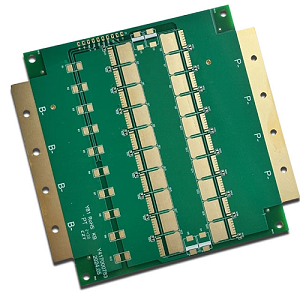
At its core, embedded copper technology is all about strategic thermal management. By embedding copper blocks in localized regions of the PCB, the heat from components in contact with these blocks is quickly conducted away, preventing overheating and ensuring the reliable operation of the electronic device. Embedded copper technology comes in two main types:
- Through – embedded type: As the name suggests, this type involves embedding the copper block completely through a certain section of the board, creating a direct thermal path through that part of the PCB structure.
- Semi – embedded type: Here, the copper block is only partially embedded into the board, still enabling effective heat transfer but with a different structural integration compared to the through-embedded type.
Key Parameters and Characteristics
To ensure the successful implementation of buried embedded technology, several key parameters and characteristics must be considered.
Copper Thickness
The thickness of the red copper used in buried copper applications varies to meet different thermal and structural needs. Common thicknesses include 0.5mm, 0.6mm, 0.8mm, 1.0mm, 1.2mm, 1.6mm, 1.8mm, 2.0mm, 2.5mm, 3.0mm, 3.2mm, and 3.5mm.
Copper Block Thickness Capability
The normal thickness of the buried copper block is ≥1.0mm, with an extreme minimum thickness of 0.5mm. If the copper block thickness is less than 1.0mm, an unconventional review is required to assess the feasibility and potential challenges.
Relationship Between Copper Block Thickness and Grooved Materials
The thickness of the copper block is closely related to the combined thickness of the grooved prepreg (PP) and grooved core board:
- For red copper with a thickness of 0.5-0.6mm, the copper block thickness is equal to the combined thickness of the grooved PP and grooved core board.
- For 0.8mm red copper, the copper block thickness is 0-0.05mm thicker than the combined thickness of the grooved PP and grooved core board.
- For red copper with a thickness of ≥1.0mm, the copper block thickness is 0.05 – 0.1mm thicker than the combined thickness of the grooved PP and grooved core board.
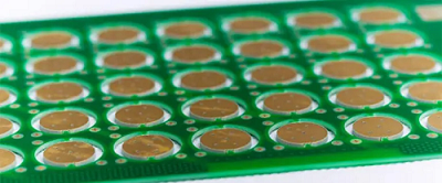
Copper Block Dimensions
The normal size of the embedded copper block is ≥3x3mm, with an extreme minimum size of 2.5×2.5mm. This ensures that the copper block can effectively perform its thermal conduction function while fitting into the PCB design.
PP Material Requirements
- At least 2 sheets of interlayer PP should be used, and priority is given to PP with a high resin content. If the board thickness allows, it is best to use 2 sheets of 1080 PP with high resin content, and it can also be mixed with 106, 3313, 2116, and 7628 PP.
- The commonly used PP material is FR-4. For special board materials such as TU-872SLK/M6/SH260/FR-27/FR-28, unconventional review and verification of the PP are required.
- Additionally, the prepreg cannot use Rogers4450F, as this type of PP has poor fluidity, making it difficult to fill the gaps of the embedded copper, and the bonding force between the PP and red copper is relatively weak
What Industries Use Embedded Copper Technology?
Embedded copper technology, valued for its strong heat dissipation, is widely used in industries requiring effective PCB thermal management. Here are key application areas:
Telecommunications
High-power devices like 5G base stations and routers generate much heat. Embedded copper in their PCBs prevents overheating, ensuring stable signal transmission and equipment longevity.
Automotive Electronics
Modern cars, especially EVs, have heat-generating systems like ECUs, ADAS, and powertrains. Embedded copper PCBs manage this heat, boosting efficiency and reliability, e.g., ensuring accurate ECU operation for better fuel efficiency.
Industrial Automation
Robotics, PLCs, and motor drives in factories run continuously, producing significant heat. Buried copper keeps temperatures in check, ensuring consistent performance and reducing downtime, like enabling precise robotic arm movements.
Medical Devices
High-power medical equipment (MRI, CT scanners) needs reliable components. Buried copper in their PCBs dissipates heat efficiently, preserving device accuracy and safety for diagnostics and treatments.
What is the Difference between Embedded Copper Technology and Embedded Copper Coin Technology?
While both embedded copper technology and embedded copper coin technology aim to improve thermal and electrical performance in PCBs, they differ in structure, purpose, and manufacturing approach. These differences affect how each is used in real-world applications, especially where high power or efficient heat transfer is needed. Understanding these distinctions can help you choose the right solution for your specific design requirements. Key Points for Understanding the Differences:
- Construction Method:
- Embedded copper uses etched copper patterns within PCB layers.
- Embedded copper coin involves physically inserting a solid copper piece into a cavity in the PCB.
- Thermal Efficiency:
- Copper coin technology offers better localized heat dissipation due to the solid metal insert.
- Embedded copper layers dissipate heat over a wider area but are less efficient for hotspots.
- Material Usage:
- Copper coin PCBs use more copper material per unit and may require custom milling and placement techniques.
- Electrical Performance:
- Both methods enhance current capacity, but embedded copper coin PCBs can handle very high current due to the solid insert.
- Manufacturing Challenges:
- Embedded copper coin PCB manufacturing needs precise cavity creation, bonding, or soldering, while embedded copper PCBs rely more on layer alignment and lamination.
- Cost Impact:
- Embedded copper coin PCBs are generally more expensive due to the complexity of coin placement and material cost.
- Application Suitability:
- Choose embedded copper technology for compact, high-layer PCBs needing better current paths.
- Opt for embedded copper coin technology when you need extreme thermal management in power-dense areas.
| Item | Embedded Copper Technology | Embedded Copper Coin Technology |
|---|---|---|
| Copper Form | Thin copper trace or layer | Solid copper coin or insert |
| Main Function | Better current flow | Better heat dissipation |
| Current Capacity | High | Very High |
| Thermal Performance | Good | Excellent |
| Cost | Medium | High |
| Used In | Power PCBs, converters | LED PCBs, IGBT boards |
What is the Embedded Copper Technology Price?
The cost of embedded copper technology depends on several factors such as copper thickness, PCB layer count, design complexity, and production volume. Since this technology involves specialized lamination and precision copper embedding, it is more expensive than standard PCBs but generally more affordable than embedded copper coin PCBs. Key Pricing Factors:
- Copper Thickness:
Thicker copper (e.g., 4 oz or more) raises the cost due to material use and processing difficulty. - PCB Layer Count:
Multilayer PCBs (e.g., 6–12 layers) are more expensive due to complex lamination steps. - Board Size & Shape:
Larger boards or irregular shapes may require special tooling, increasing cost. - Design Complexity:
PCBs with tight tolerances or dense copper patterns need more precise manufacturing, which adds cost. - Surface Finish & Materials:
Using high-grade materials like Rogers, ceramic, or high-Tg FR4 increases the base price. - Volume & Lead Time:
Higher quantities usually get volume discounts. Rush orders may incur a premium.
Finally, for accurate pricing, it’s best to request a custom quote from a reliable copper coin PCB manufacturer. Sharing detailed Gerber files, copper thickness requirements, and order quantity helps the supplier provide precise cost estimates.
How to Control the Quality of Embedded Copper PCB?
Quality control is critical in the production of Embedded Copper PCBs because even small defects can affect performance, especially for high-current or thermal-sensitive applications. To ensure reliable function and long service life, manufacturers must follow strict processes during every step of production. Key Steps to Control Quality:
- Design Verification
- Confirm the design files (Gerber, drill, stack-up) are correct.
- Check copper thickness and embedding depth specifications.
- Run DFM (Design for Manufacturability) checks before fabrication starts.
- Material Inspection
- Verify incoming copper sheets for purity and uniform thickness.
- Check base material (e.g., FR4, ceramic) for quality certifications.
- Use only approved vendors for key materials.
- Precision Copper Embedding
- Ensure accurate alignment during lamination.
- Monitor lamination pressure and temperature to avoid voids or delamination.
- Use CNC milling or laser drilling for high accuracy when creating cavities or channels for copper.
- Bonding and Plating Quality
- Inspect the bonding between embedded copper and the surrounding dielectric.
- Ensure proper copper plating in vias and around embedded sections.
- Control surface finish (ENIG, HASL) thickness and uniformity.
- Thermal Management Testing
- Use thermal imaging to check heat distribution.
- Verify thermal conductivity using standardized tests.
- Simulate working conditions to validate heat dissipation.
- Electrical Testing
- Perform 100% electrical testing for opens and shorts.
- Measure resistance of copper paths, especially around embedded areas.
- Test high-current performance to ensure no overheating or voltage drop.
- X-ray and AOI Inspection
- Use X-ray inspection to detect hidden defects under embedded copper.
- Apply Automated Optical Inspection (AOI) for visual defects such as misalignment or cracks.
- Mechanical Stress Testing
- Conduct flex and vibration tests for mechanical reliability.
- Test peel strength of copper to ensure it is securely embedded.
- Final Quality Assurance (QA)
- Check against IPC standards (e.g., IPC-6012 for rigid PCBs).
- Document inspection reports and traceability through MES systems.
- Conduct final visual and functional tests before shipment.
In summary, controlling the quality of Embedded Copper PCBs requires a mix of advanced equipment, skilled engineering, and strict inspection standards. From design verification to final testing, every step must be carefully monitored. Choosing a reliable manufacturer with strong quality systems ensures consistent performance and long-term reliability in demanding applications.
Why Choose EBest Circuit (Best Technology) for Manufacturing Embedded Copper PCB and Copper Coin PCB?
Choosing the right manufacturer for Embedded Copper PCB and Embedded Copper Coin PCB is essential for ensuring product performance, durability, and timely delivery. EBest Circuit (Best Technology) stands out as a professional and dependable partner for demanding PCB projects. Here’s why many global customers trust us:
1. Professional Engineering Support
Our experienced engineers work closely with you from design review to prototype testing. We offer expert guidance on copper thickness selection, embedding depth, and thermal management to help you get the most out of your design.
2. Advanced Manufacturing Equipment
We use high-precision CNC machines and laser systems for copper cavity processing, ensuring tight tolerances and reliable copper placement. Our modern lamination and plating lines guarantee high-quality bonding and finish.
3. Strict Quality Control Systems
Quality is our top priority. We follow ISO9001, IATF16949 for automotive, ISO13485 for medical, and AS9100D for aerospace standards. We implement rigorous QC inspection after each manufacturing step.
4. Fast Turnaround Time
With optimized workflows and flexible production lines, we can deliver both prototypes and mass production orders quickly. Our on-time delivery rate consistently exceeds 97%.
5. Flexible MOQ
Whether you require a small batch or a large volume, we are always available to assist you. For a small prototype, it is beneficial for startups and R&D projects.
6. Wide Material Selection
We offer a variety of base materials including FR4, Rogers, ceramic substrates, and more. For copper coins, we support custom sizes and shapes, and ensure the thermal and electrical specs match your exact requirements.
7. Extensive Experience with High-Power Applications
EBest Circuit (Best Technology) has completed hundreds of projects involving embedded copper and copper coin PCBs for applications like power converters, LED lighting, IGBT modules, and automotive power control units. We have specific experience to present a practical solution for you.
8. One-Stop Service
From PCB fabrication to assembly and testing, we offer a full range of services under one roof. This reduces lead times and helps avoid delays or quality mismatches between different vendors.
To sum up, When you work with EBest Circuit (Best Technology), you get more than a PCB supplier — you gain a reliable partner dedicated to quality, speed, and customer success. For high-current or thermal-critical designs, our Embedded Copper PCB and Copper Coin PCB solutions provide the performance and reliability your project demands.
In a nutshell, embedded copper technology offers a reliable and efficient solution for thermal management in PCB design. By understanding its processes, parameters, and material requirements, manufacturers can produce high-performance PCBs that meet the demanding heat dissipation needs of your product application. If you have any other questions, just feel free to contact us at sales@bestpcbs.com any time!