

A Cu inlay PCB, also called copper inlay PCB or bus bar PCB, is designed to manage high current flow and heat dissipation in modern electronic systems. As electronic devices become more compact and powerful, the need for better power handling within limited space grows rapidly. Standard copper traces often can’t handle high current without overheating or losing efficiency. That’s where copper inlay PCBs offer a smart and effective solution.
At EBest Circuit (Best Technology), we specialize in custom copper inlay PCBs, supporting demanding industries like automotive, industrial control, and renewable energy. We use advanced techniques to embed copper bars directly into PCBs, helping your products perform better and last longer.
What Is Cu Inlay PCB?
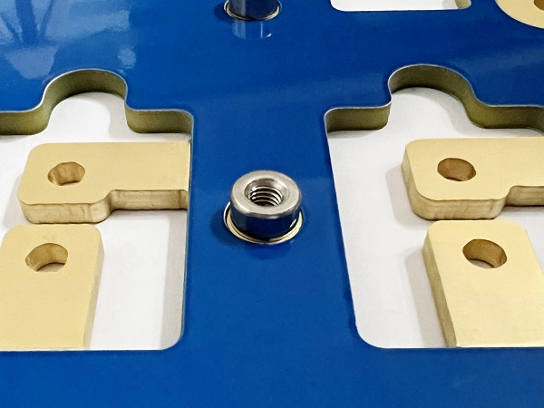
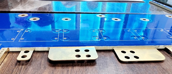
A Cu inlay PCB is a circuit board where solid copper blocks or bars are inserted into the board structure. These copper inlays are physically placed into slots or cutouts in the base material of the PCB, often FR4, aluminum, or other substrates.
The copper inlay becomes part of the circuit, connecting to surrounding copper traces and components. Instead of relying on thin copper layers, which might struggle with high current, thick copper inlays offer a low-resistance path for electricity and a direct route for heat dissipation.
These PCBs are sometimes known as bus bar PCBs because the inlay acts like a mini bus bar embedded inside the board. They are often found in designs where power density is high, and the space for external power routing is limited.
What Is the Working Principle of Inlay Copper in PCB?
In a copper inlay PCB, the working principle revolves around using solid copper bars to conduct electricity and transfer heat efficiently. Here’s how it works:
- Precision Cutouts: During the PCB manufacturing process, slots or grooves are milled into the base material to fit the copper inlays.
- Copper Insertion: A solid copper bar or block is placed into each slot, making it part of the board structure.
- Electrical Connection: The inlay is then electrically connected to surrounding copper traces. This can be done via plated-through holes, soldering, or lamination, depending on the design.
- Heat Transfer: When high current flows through the board, the copper inlay not only carries the current but also absorbs and spreads heat. This helps prevent overheating and improves the reliability of the entire system.
Because copper has high electrical and thermal conductivity, the inlay serves two purposes: reducing voltage loss and keeping temperatures low.
Why Inlay Copper in the PCB?
The main reason to use inlay copper in a PCB is to manage high current and heat in a compact space. In many power electronic devices, standard copper layers are too thin to carry heavy current without voltage drops or overheating. Here are key reasons to choose copper inlay PCB:
- High Current Needs: When your design must carry more than 20-100 amps of current, copper inlays provide a path that minimizes power loss.
- Thermal Control: Devices with power-hungry components, such as power MOSFETs, IGBTs, or coils, generate a lot of heat. Copper inlays help pull heat away from these hot spots.
- Space Limitations: Using thick copper over the entire PCB increases cost and thickness. Copper inlay allows selective reinforcement, only where needed.
- Improved Design Flexibility: Copper inlays can be designed into specific regions, enabling multi-zone current paths and optimized thermal management.
In short, inlay copper in PCB helps engineers create more reliable, efficient, and compact systems.
Benefits of Copper Inlay PCB
1. With a copper inlay, your PCB can safely carry high current levels (often over 100A) without the risk of burning or damage. The solid copper inlay has low resistance, which minimizes energy loss.
2. Copper inlays absorb heat from nearby components and transfer it efficiently to heat sinks or metal housings.
3. Instead of using bulky external bus bars or thick copper layers, copper inlays offer a space-saving option. They let you design smaller PCBs with higher performance, which is ideal for portable or space-constrained products.
4. The solid metal insert adds strength to the PCB structure. It prevents board bending or warping and supports heavy components mounted on top.
Copper Core PCB vs Copper Inlay PCB
Some engineers may wonder: should I choose copper core PCB or copper inlay PCB? Both types are designed to improve heat management and electrical performance, but they use different structures and serve different needs.
A copper core PCB is a type of metal core PCB, uses a solid copper plate as the base material. This copper core acts as a heat spreader, helping to quickly transfer heat away from the entire board. It is ideal for applications where even heat distribution is required across a large area.
In contrast, a copper inlay PCB typically uses FR4 or other insulating materials as the base, with copper bars inserted into machined slots only in selected areas. These copper inlays handle high current directly and provide localized thermal management exactly where it’s needed.
| Feature | Copper Core PCB | Copper Inlay PCB |
| Copper Placement | Full copper plate inside the PCB | Copper bar inserted into slots |
| Heat Management | Uniform heat spread across the board | Targeted heat dissipation |
| Current Handling | Good, but may require thick PCB | Excellent, at specific points |
| Flexibility in Design | Less flexible, fixed copper plate | Flexible, inlays only where needed |
| Cost | Higher due to full copper layer | More cost-effective (selective use) |
In summary, copper core PCBs are best for broad heat dissipation, while copper inlay PCBs are preferred when you need high current capacity in specific zones with better design flexibility and material savings.
Factors Affect Copper Inlay PCB Price
The price of copper inlay PCBs can vary widely based on your design needs, order volume, and technical requirements. Several factors directly affect the cost:
1. Copper Inlay Size and Thickness
Larger and thicker copper bars increase both material and machining costs. Inlays typically range from 1mm to 5mm thick. Thicker copper costs more due to higher copper usage and longer machining time.
2. Board Size and Layers
Larger PCBs and multi-layer designs involve more material, labor, and processing steps, leading to higher costs.
3. Surface Finishes and Testing
Special surface finishes like ENIG, immersion silver, or selective gold plating, as well as full electrical or thermal testing, can add to the overall cost.
4. Order Quantity
Larger orders benefit from volume discounts, while small batches have higher unit prices due to setup and tooling time.
5. Price Range
For reference, the typical price range for copper inlay PCBs is approximately:
- Prototype or low volume: $300 – $800 per square meter
- Medium volume: $200 – $400 per square meter
- Mass production: $100 – $250 per square meter
Note: These are estimated ranges. Actual prices depend on copper inlay dimensions, layer count, complexity, and finish options.
Applications of Inlay Copper PCB
Copper inlay PCBs are found in various high-performance industries. They are ideal for power electronics, where current and thermal reliability are critical.
Here are typical applications:
- Electric Vehicles (EV): Power inverters, charging systems, battery control units.
- Industrial Equipment: Motor drives, programmable logic controllers (PLCs), industrial inverters.
- Renewable Energy Systems: Solar panel controllers, wind turbine systems, energy storage units.
- Telecommunication: Base station power modules, signal amplifiers.
- Medical Devices: MRI machines, laser equipment, diagnostic tools needing high power.
- Aerospace: Avionics systems requiring compact, high-current PCBs.
Wherever power density and space-saving are essential, copper inlay PCBs provide a robust solution.
Copper Inlay PCB Market Trend
The global copper inlay PCB market is experiencing steady growth. As industries demand higher efficiency and miniaturization, copper inlay PCBs are becoming a preferred solution.
Key market trends include:
- Rapid growth in electric vehicles, where compact power modules are essential.
- Expansion in solar and wind energy sectors, requiring efficient power conversion.
- Increased use of AI and 5G equipment, which needs reliable power systems.
- Rising demand for high-performance PCBs in medical, defense, and aerospace applications.
As a leading copper inlay PCB manufacturer, EBest Circuit (Best Technology) continues to invest in production capacity, quality systems, and engineering services to meet this rising demand.
Why Choose EBest Circuit (Best Technology) for Your Copper Inlay PCBs?
With over a decade of experience in advanced PCB manufacturing, EBest Circuit (Best Technology) is a trusted partner for companies needing high-performance copper inlay PCBs. We’ve helped clients in automotive, industrial control, telecommunications, and energy sectors bring reliable products to market faster.
1. We have extensive experience producing copper inlay PCBs with varied designs—from simple one-inlay boards to complex multi-inlay configurations.
2. Our production lines feature state-of-the-art CNC milling equipment, automated plating systems, and tight-tolerance inspection tools.
3. Our R&D team and senior engineers work directly with clients to optimize designs, suggest improvements, and solve complex challenges.
4. With efficient production scheduling, MES-based traceability, and streamlined logistics, we deliver both prototypes and volume orders quickly.
5. We are certificated with ISO9001, IATF16949, ISO13485, AS9100D systems.
FAQs
1. What is the typical thickness of copper inlays?
They usually range from 1mm to 5mm, depending on current needs.
2. Can copper inlays be used in multi-layer PCBs?
Yes, with proper planning, copper inlays can be included in multi-layer designs.
3. How are copper inlays secured to the board?
Inlays are typically bonded using lamination, plating, or soldering.
4. What current can a copper inlay PCB handle?
With proper design, it can handle 100A or more safely.
5. Are copper inlay PCBs better than thick copper PCBs?
For localized high current and heat, yes. Copper inlays offer better efficiency and design flexibility.
If you’re looking to upgrade your PCB design with copper inlays for better performance and reliability, contact EBest Circuit (Best Technology) today. Our team is ready to help with design consultation, sample production, and mass manufacturing. Get a custom copper inlay PCB quote today!
Tags: copper inlay pcb market, copper inlay pcb, Cu Inlay PCB, pcb copper inlay