

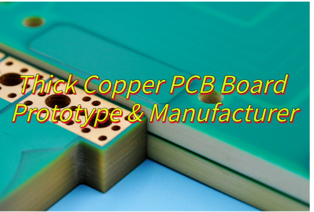
Looking for thick copper PCB solution? This guide explores its benefits, application, specifications, manufacturing advantages, manufacturing process..
- Struggling with frequent PCB failures due to overheating in high-current designs?
- Need thicker copper for power integrity but worried about manufacturing defects?
- Tired of suppliers charging premium prices for 6oz+ copper boards with slow turnarounds?
EBest Circuit (Best Technology) Can Provide:
- Robust Thermal Management: Advanced 4oz–15oz copper plating ensures 30%+ heat dissipation, reducing hotspots in power electronics.
- Zero-Defect Fabrication: Laser-drilled vias and symmetrical stacking prevent copper peeling, even in multilayer designs.
- Cost-Efficient Scaling: Optimized panel utilization and bulk-order discounts cut costs by 15% without sacrificing quality.
Welcome to contact EBest Circuit (Best Technology): sales@bestpcbs.com.
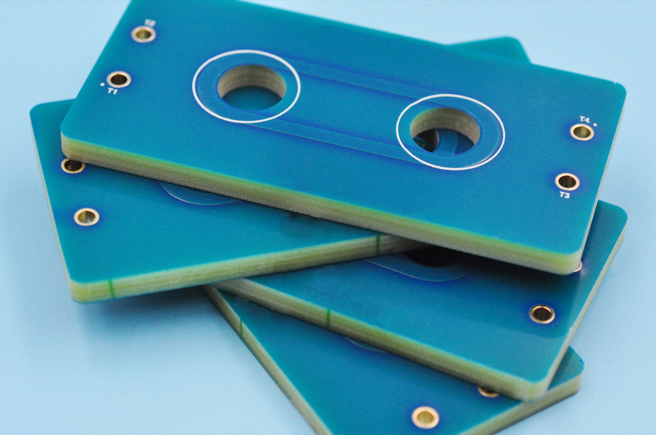
What Is Thick Copper PCB?
Thick copper PCB, often termed heavy copper PCB, is a specialized printed circuit board featuring copper layers substantially thicker than standard designs, usually exceeding 3 ounces per square foot (approximately 105 micrometers), to support elevated electrical loads and thermal dissipation.
This design significantly boosts current-carrying capacity, minimizes resistance, and enhances reliability in high-power environments like industrial equipment, automotive systems, and renewable energy applications, where heat management and durability are prioritized.
Heavy Copper PCB Specification
| Category | Specification |
| Copper Weight | 3 oz/ft² (105 µm) to 20 oz/ft² (700 µm) or custom thicknesses. |
| Current Capacity | Supports 100A+ with proper trace design; reduces resistive power loss. |
| Thermal Management | High thermal conductivity (385 W/m·K) for effective heat dissipation. |
| Dielectric Material | FR-4, polyimide, or ceramic substrates compatible with thick copper layers. |
| Minimum Trace Width | 0.3–0.5 mm (varies with copper weight and etching process). |
| Plating Requirements | Additional copper plating (up to 5 oz) for vias/pads to prevent cracking. |
| Aspect Ratio | 8:1 (drill depth to diameter) for reliable through-hole plating. |
| Finish Options | HASL, ENIG, immersion silver, or selective gold plating for corrosion resistance. |
| Operating Temperature | -50°C to +150°C (material-dependent). |
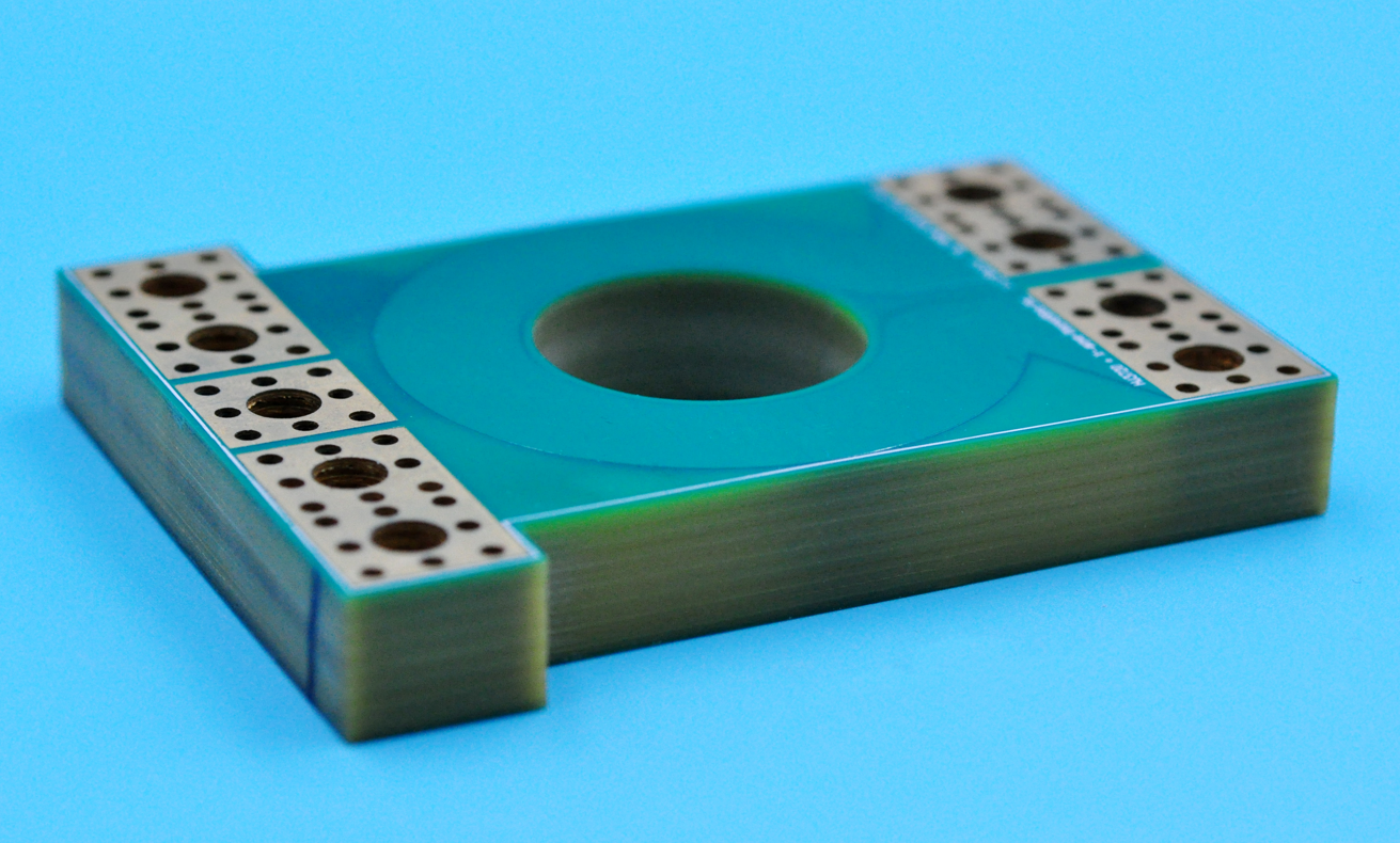
Benefits of Thick Copper PCB Board
- Enhanced Current-Carrying Capacity – Thick copper layers (3 oz/ft² to 20+ oz/ft²) reduce electrical resistance, enabling higher current flow without overheating. Ideal for power converters and motor drives.
- Superior Thermal Management – Increased copper mass dissipates heat efficiently, minimizing hot spots in high-power applications like industrial machinery or EV charging systems.
- Improved Mechanical Durability – Resists thermal expansion stress and vibration, extending lifespan in harsh environments (e.g., aerospace, automotive).
- Space Optimization in Complex Designs – Combines high-power traces with standard circuits on a single board, reducing assembly size and simplifying layouts.
- Higher Reliability Under Extreme Conditions – Stable performance in high-temperature or high-voltage scenarios, such as renewable energy inverters or defense systems.
- Reduced Power Loss – Lower resistive losses compared to thin-copper alternatives, enhancing energy efficiency in data centers and telecom infrastructure.
- Flexible Design Integration – Supports mixed-technology designs (e.g., embedded components) for advanced electronics requiring both signal integrity and power delivery.
- Cost-Effective for High-Power Applications – Long-term savings by reducing the need for additional cooling components or redundant circuitry.
Application of Thick Copper PCBs
- Power Electronics – High-current inverters, DC-DC converters, industrial power supplies (currents >50A).
- Automotive Systems – Electric vehicle battery management systems, onboard chargers, traction motor controllers (vibration, thermal cycling).
- Renewable Energy Infrastructure – Solar inverters, wind turbine converters, grid-tied energy storage systems (high-current flows, outdoor thermal loads).
- Industrial Machinery – Motor drives, welding equipment, automation controllers (surge currents, repetitive thermal stress).
- Aerospace and Defense – Avionics power systems, radar transmitters, satellite communication modules (vacuum, radiation, mechanical shock).
- High-Power LED Lighting – Stadium lighting arrays, horticultural grow lights, automotive headlamp systems (uniform heat distribution across LED arrays).
- Medical Devices – MRI cooling systems, laser surgery equipment, diagnostic imaging power modules (stable power delivery, sterile environments).
Manufacturing Processes of Thick Copper PCB Board
1. Design Preparation: Use CAD software to define circuit patterns, ensuring trace widths and spacing comply with thick copper (≥3 oz/ft²) current-carrying requirements.
2. Material Selection: Choose substrates with high thermal stability (e.g., FR-4, polyimide) and copper foils tailored to target thickness (4 oz/ft² to 20 oz/ft²).
3. Copper Deposition: Apply electroplating or etched-foil processes to achieve uniform copper layers. Thick copper requires controlled plating currents to avoid voids or uneven distribution.
4. Pattern Etching: Use alkaline or acidic etchants to remove excess copper. Thick copper demands longer etching times and specialized chemistry to prevent undercutting.
5. Lamination: Stack prepreg layers and copper clads under high temperature/pressure. Thick copper boards may require sequential lamination to manage resin flow and avoid delamination.
6. Drilling: Machine-drill via holes using carbide bits. Thick copper boards need slower drill speeds and peck-drilling cycles to prevent bit wear and ensure hole quality.
7. Through-Hole Plating: Deposit copper into drilled vias via electroless or electrolytic plating. Thick copper requires thicker via barrels (≥1.5 mils) to withstand high current and thermal stress.
8. Solder Mask: Apply epoxy-based solder mask using screen printing or spray coating. Thick copper boards may need adjusted mask thickness to cover raised copper areas.
9. Surface Finish: Apply finishes like HASL (Hot Air Solder Leveling), ENIG (Electroless Nickel Immersion Gold), or OSP (Organic Solderability Preservative) for solderability and corrosion resistance.
10. Testing: Perform electrical continuity tests, thermal cycling, and impedance checks to validate performance under high-current and high-temperature conditions.
Why Choose EBest Circuit (Best Technology) as Thick Copper PCB Manufacturer?
Reasons why choose EBest Circuit (Best Technology) as your thick copper PCB manufacturer:
- Proven Expertise in Thick Copper (4–20 oz/ft²) Applications: Leverage specialized knowledge in high-power PCB design to avoid common pitfalls and ensure performance.
- One-Stop Solution from Design to Delivery: Streamlines project management by consolidating prototyping, fabrication, and assembly under one roof.
- 48-Hour Rapid Prototyping Delivery: Accelerates product development cycles, enabling faster time-to-market and competitive edge in high-demand industries.
- Certified Compliance (ISO 9001, UL, RoHS, ISO 9001, IATF 16949 ): Mitigates regulatory risks and ensures products meet global standards for safety and environmental compliance.
- Stringent Quality Control with 100% Inspection: Eliminates hidden defects, reduces rework costs, and ensures reliability in high-current/thermal applications.
- Transparent Pricing with No Hidden Fees: Predictable budgeting and cost savings through upfront pricing models tailored to thick copper PCB specifications.
- Free DFM (Design for Manufacturability) Analysis: Optimizes PCB layouts to reduce material waste, lower production costs, and avoid late-stage design revisions.
- 24/7 Dedicated Engineer Support Team: Instant technical guidance for complex thick copper designs, troubleshooting, and process optimization.
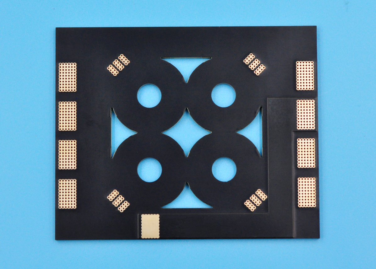
Our Thick Copper PCB Capabilities
| Base material | FR4/Aluminum |
| Copper thickness | 4 OZ~10 OZ |
| Extreme Heavy Copper | 20~200 OZ |
| Outline | Routing, punching, V-Cut |
| Soldermask | White/Black/Blue/Green/Red Oil |
| Surface finishing | Immersion Gold, HASL, OSP |
| Max Panel size | 580*480mm(22.8″*18.9″) |
Thick Copper PCB Board Prototype Fast Delivery
Standard Lead Time (Conventional Processes)
- Single/Double Layers: Delivery within 3 business days (supports ≤1.5OZ copper thickness)
- 4-6 Layers: Completion in 5 business days (supports ≤3OZ copper + resin plugging)
Expedited Service (Additional Cost Applies)
- 48-Hour Rush: For ≤4-layer boards, copper ≤4OZ (file feasibility must be confirmed in advance)
- 72-Hour Priority: Covers 6-layer thick copper boards (including impedance control)
Extended Time for Special Processes
- Extra-Thick Copper (≥6OZ): Standard lead time + 1-2 days (requires extended plating time)
- Hybrid Lamination (e.g., aluminum substrate): Lead time increased by 30% (quoted separately)
How to Get A Quote for Thick Copper PCB Boards?
Here are essential files to submit your heavy copper PCB manufacturer:
- Gerber Files: Provide complete PCB design files in standard Gerber format for fabrication.
- Bill of Materials (BOM): Include a detailed BOM list with component specifications, quantities, and reference designators.
- Assembly Drawings: Submit clear assembly diagrams or schematics to guide manufacturing.
- Additional Specifications: Clearly state copper thickness (e.g., 3OZ, 4OZ or higher), layer count, and any special processes like resin plugging or impedance control.
- Sample PCB or PCBA (Optional): Sending a physical sample can help verify complex designs and improve quote accuracy.
For customized quotes and expert support on thick copper boards, please contact EBest Circuit (Best Technology) directly. Submit your files via email for a response within hours: sales@bestpcbs.com.