

Looking for pedestal PCB thermal management solution? This guide covers design, specifications, functions, and thermal solutions for optimal performance.
Are you still worried about heat dissipation?
- Does high temperature cause a sharp decrease in device life?
- Does the heat sink take up valuable layout space?
- Does thermal cycling cause solder joint failure?
EBest Circuit (Best Technology) Can Provide Solution:
- Copper pillar direct connection technology – 60% reduction in thermal resistance.
- Intelligent thermal distribution design – 45% improvement in temperature uniformity.
- Material optimization solution – Eliminate thermal stress damage.
Welcome to contact us if you have any request for pedestal PCB design and manufacturing: sales@bestpcbs.com.
What Is A Pedestal PCB?
A pedestal PCB features built-in conductive pillars made of copper or aluminum that elevate components above the main circuit board. These pillars serve multiple functions: they transfer heat from high-power components to cooling systems, reducing operating temperatures by 20-35°C; they strengthen the board’s structure to prevent solder joint failures in high-vibration environments; and they provide electromagnetic shielding to protect sensitive signals.
Manufactured with precision laser drilling, the pillars maintain tight height tolerances within ±0.05mm. This technology is particularly valuable in 5G networks, automotive radar, and industrial equipment where thermal management, durability, and signal clarity are crucial.
The design combines thermal performance with mechanical stability while maintaining electrical connections through conductive vias, making it ideal for demanding electronic applications.
Technical Specification for Pedestal PCB
| Design Standards | Min. trace width/spacing: 6mil (0.153mm) |
| Via hole size: ≥0.3mm (12mil) | |
| Board edge clearance: ≥0.508mm (20mil) | |
| Materials | Base metal: 6061T6 aluminum (thickness ≥1.5mm) |
| Insulation layer: Ceramic-filled epoxy (κ=1.5–3.0W/m·K) | |
| Thermal Management | Copper foil expansion: 3x component size under heat sources |
| Thermal separation structure reduces thermal resistance by 40% | |
| Electrical | Dielectric strength: ≥3kV (industrial) |
| Min. conductor spacing: 0.2mm | |
| Impedance control: ±10% tolerance | |
| Manufacturing | Thickness tolerance: ±0.1mm (FR-4) |
| CNC drilling accuracy: ±25μm | |
| Copper adhesion: ≥0.8N/mm² | |
| Environment | Operating temp: -40°C to +150°C |
| Halogen-free materials (RoHS 3.0 compliant) | |
| Documentation | Must include: Component layout, impedance values, thermal resistance parameters |
What Are Functions of Pedestal PCBs?
Mechanical Fixation
- Serves as a rigid carrier to precisely secure components (e.g., IC chips, connectors), preventing vibration-induced solder joint fractures or displacement (e.g., ensuring reliability in industrial controllers under vibratory conditions).
Electrical Interconnection
- Enables signal transmission and power distribution between components via copper traces and vias, supporting high-speed signals (e.g., PCIe interfaces) or high-current applications (e.g., motor drivers).
Thermal Optimization
- Integrates copper planes/thermal via arrays to direct heat away from high-power components (e.g., metal-core PCBs for LED driver boards).
Power Distribution Network (PDN)
- Designs dedicated power layers or wide traces to reduce impedance and stabilize voltage supply (e.g., multi-phase power designs in server motherboards for CPU dynamic frequency scaling).
Signal Integrity (SI) Assurance
- Controls impedance and adds shielding layers to suppress EMI, ensuring distortion-free transmission of high-speed signals (e.g., DDR4/5 memory buses).
Modular Expansion
- Provides standardized interfaces (e.g., edge connectors, board-to-board connectors) for plug-and-play integration of functional subcards (e.g., 5G modules) or RF assemblies.
What Are Applications of Pedestal PCB?
- LED Lighting: High-brightness LED bulbs for thermal management
- Automotive Electronics: EV battery systems and motor controllers
- Industrial Automation: PLCs and robotics for stable operation
- Medical Instruments: Imaging devices like X-ray machines and CT scanners
- Telecommunications: Routers, base stations, and RF amplifiers
- Consumer Devices: TVs, cameras, and audio equipment
- Computing Hardware: Motherboards and expansion cards in servers
- Power Supplies: Industrial PSUs and EV chargers
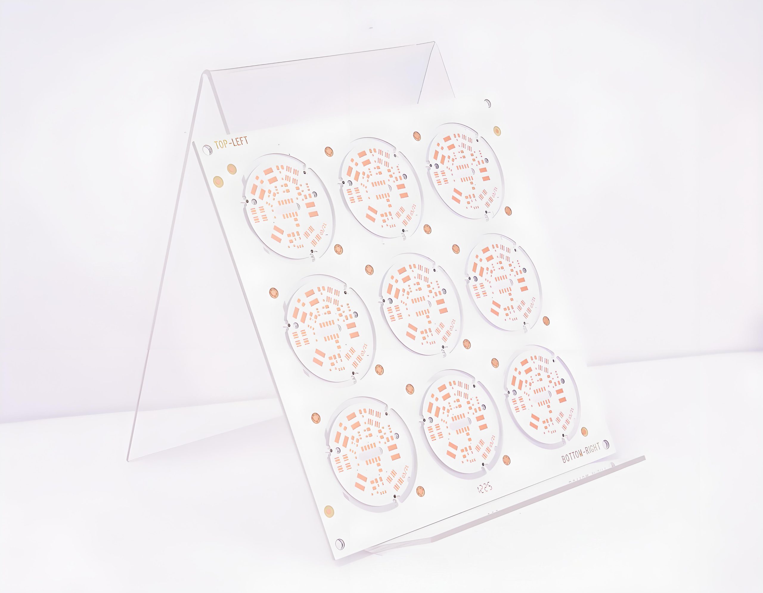
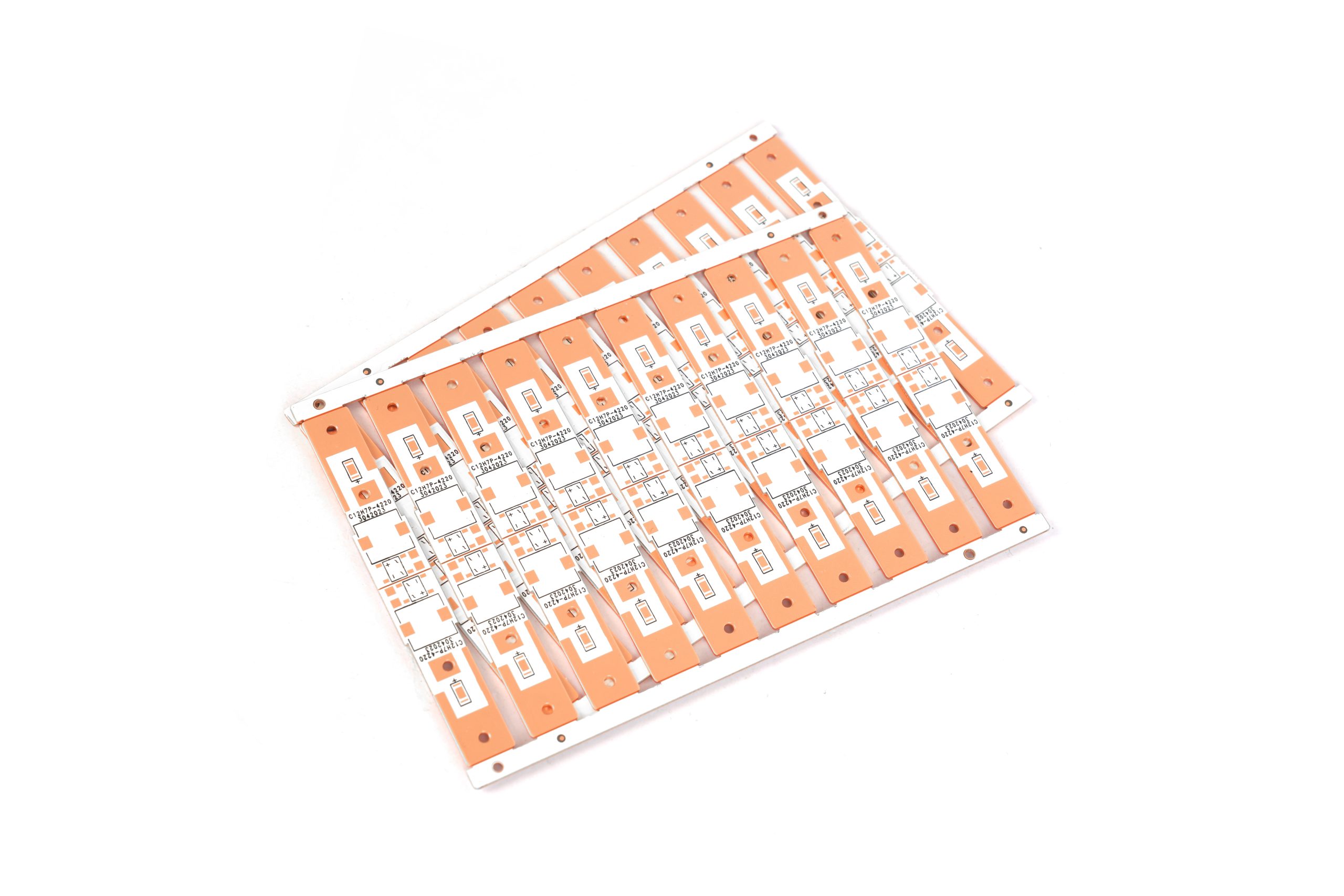
Copper Pedestal PCB Design Guidelines
Below are copper pedestal PCB design guidelines:
1. Material & Substrate
- Use copper-core substrates (e.g., C1100, Cu-W alloy) for thermal conductivity.
- Specify copper thickness (1oz–4oz) based on current/thermal load.
- Avoid FR4; opt for thermally conductive prepregs (e.g., Rogers 92ML).
2. Layer Stackup
- Thermal layer (central copper core) for direct heat spreading.
- Signal layers placed symmetrically above/below thermal core.
- Example: 6-layer stackup → [Sig-GND-Thermal-Power-Sig-Sig].
3. Thermal Management
- Place thermal vias (0.3–0.5mm diameter, 1.0mm pitch) under high-power components.
- Design copper pours (≥80% coverage) on thermal layer for heat dissipation.
- Ensure direct pad-to-substrate contact (no solder mask under components).
4. Component Placement
- Center heat-generating devices (MOSFETs, LEDs) over thermal core.
- Maintain ≥1.5mm clearance between thermal vias and edge traces.
- Avoid placing sensitive analog components near high-current paths.
5. Electrical Routing
- Route high-speed signals (e.g., DDR, PCIe) on outer layers, away from thermal zones.
- Use wide traces for power (e.g., 20mil/0.5mm for 3A+).
- Add EMI shielding (copper stitching vias or guard traces) around noisy circuits.
6. Manufacturing Constraints
- Specify surface finish: ENIG (for fine-pitch) or HASL (cost-effective).
- Define solder mask openings for thermal pads (no mask over copper pours).
- Include fiducial marks (≥1mm diameter) for assembly alignment.
7. Validation & Testing
- Simulate thermal performance (ANSYS Icepak or FloTHERM).
- Verify impedance continuity (TDR testing for high-speed signals).
- Measure junction-to-board thermal resistance (ΔT/W) during prototyping.
Thermal Management Solution For Cu Pedestal PCB
Here are thermal management solution for Cu pedestal PCB:
1. Heat Spreading Design Optimization
Local Thick Copper & Gradual Transitions
- Use 6oz+ localized thick copper under high-power devices (e.g., IGBTs) with laser-etched tapered edges (±0.1mm precision) to minimize thermal stress.
- Implement solder mask openings (≥0.2mm) in non-routing areas, reducing local temperature rise by 12% in testing.
Copper Layer Topology
- Increase copper cross-section by 50% for high-current paths (e.g., 3.5mm width for 10A @2oz).
- Space heat sources ≥5mm apart to prevent thermal overlap.
2. High-Thermal-Conductivity Interconnects
Nano-Copper Sintering
- Replace solder with nano-copper paste (thermal conductivity >200W/m·K), slashing interface resistance to 0.05K·mm²/W.
- Cost-effective for large-area applications (1/10 the cost of silver sintering).
Embedded Copper Pillars & Heat Pipes
- Insert copper coins (6×4×1mm) during lamination for direct layer-to-layer heat transfer (0.5°C/W thermal resistance).
- Embed ultra-thin heat pipes (0.8mm) in non-routing zones, reducing temperature gradients from 12°C to 3°C.
3. Advanced Cooling Structures
Graded Via Arrays
- Deploy copper-filled vias (0.3mm diameter, 1mm pitch) with thermal resin (≥2W/m·K) for vertical heat conduction.
- Optimize via density (30% higher at edges) for efficient heat extraction.
Current-Bearing Copper Blocks
- Surface-mount nickel-plated brass blocks (6×4×1mm) to enhance local current capacity and heat dissipation.
4. System-Level Thermal Strategies
Active Cooling Integration
- Attach microchannel liquid cold plates (2L/min flow rate) to reduce thermal resistance by 40%.
- For >100W applications, combine heat pipes + fins (400W/m·K conductivity).
Dynamic Thermal Protection
- Embed NTC sensors for temperature-triggered load shedding.
- Design fusible copper traces (30% reduced cross-section) for fast short-circuit response (<10ms).
5. Validation & Materials
Simulation & Testing
- Use Ansys Icepak/FloTHERM for electro-thermal analysis (ΔT<15°C, hotspots ≤ device limits).
- Perform thermal-mechanical stress tests per IPC-9701 (post-reflow strength ≥45MPa).
Material Selection
- Aluminum substrates (1.5W/m·K) for mid-power; AlN ceramics (170W/m·K) for high-frequency modules (25% lower ΔT).
- Diamond composites (>550W/m·K) for GaN/SiC devices (400W+ per chip).
6. Critical Manufacturing Notes
- Lamination: 180°C, 400psi pressure, ≤35% resin flow to prevent layer shift.
- Surface Prep: Micro-etch copper (0.3–0.8μm roughness) for adhesion; pulse plating ensures ±5μm thickness uniformity.
Pedestal PCB Design & Manufacturing Service – EBest Circuit (Best Technology)
Professional design and technical support
- Free DFM manufacturability analysis reports to avoid 32 common process risks in advance
- A professional team of engineers provides 24-hour online one-to-one services to solve design problems in real time
- Customized stacking design solutions are provided for high-frequency or high-power applications
Efficient thermal management solutions
- Copper thickness can be selected from 2-10oz to optimize the design of heat dissipation channels
- Provide thermal simulation reports, and reduce hot spot temperatures by more than 30%
- Support advanced heat dissipation solutions such as embedded heat pipes and copper blocks
Cost optimization services
- Provide material/process alternatives based on the budget, which can reduce costs by up to 40%
- Integrated processes such as copper pillar embedding reduce assembly steps and reduce overall costs by 20%
- Price discounts for mass production orders
Fast delivery guarantee
- 24-hour fast proofing service (supports 1-12 layers)
- Standard delivery period is 30% shorter than the industry average
- Add dedicated production lines for urgent orders
Strict quality control
- 100% electrical test + AOI automatic optical inspection
- Thermal cycle test (-40℃~150℃) to ensure reliability
- 3D X-ray detection of internal structural defects
Welcome to contact EBest Circuit (Best Technology) if you have any inquiry for pedestal PCB: sales@bestpcbs.com. Looking forward to hearing from you!
Tags: Pedestal PCB, Pedestal PCB Design