

Are you worried about how to choose PCB copper thickness? Let’s master PCB copper thickness selection to optimize circuit performance, current handling, and thermal reliability with this comprehensive guide.
Are you troubled by these problems?
- Uneven copper thickness leads to impedance loss? How to ensure high-frequency signal integrity?
- Copper foil bubbles and falls off in high current scenarios? How to achieve both heat dissipation and reliability?
- Copper thickness deviation exceeds 5% after lamination of multilayer boards? How to control mass production consistency?
The Solution EBest Circuit (Best Technology) Can Provide:
- Laser thickness measurement + dynamic compensation system – real-time control of etching parameters, copper thickness tolerance ±1.5μm.
- Patented browning process – copper surface bonding strength increased by 60%, passed 3×288 hours salt spray test.
- Full process thickness traceability – 20 parameters are recorded independently for each layer of board, and CPK value is stable ≥1.67.
Welcome to contact us if you have any request for PCB design, manufacturing or assembly service: sales@bestpcbs.com.
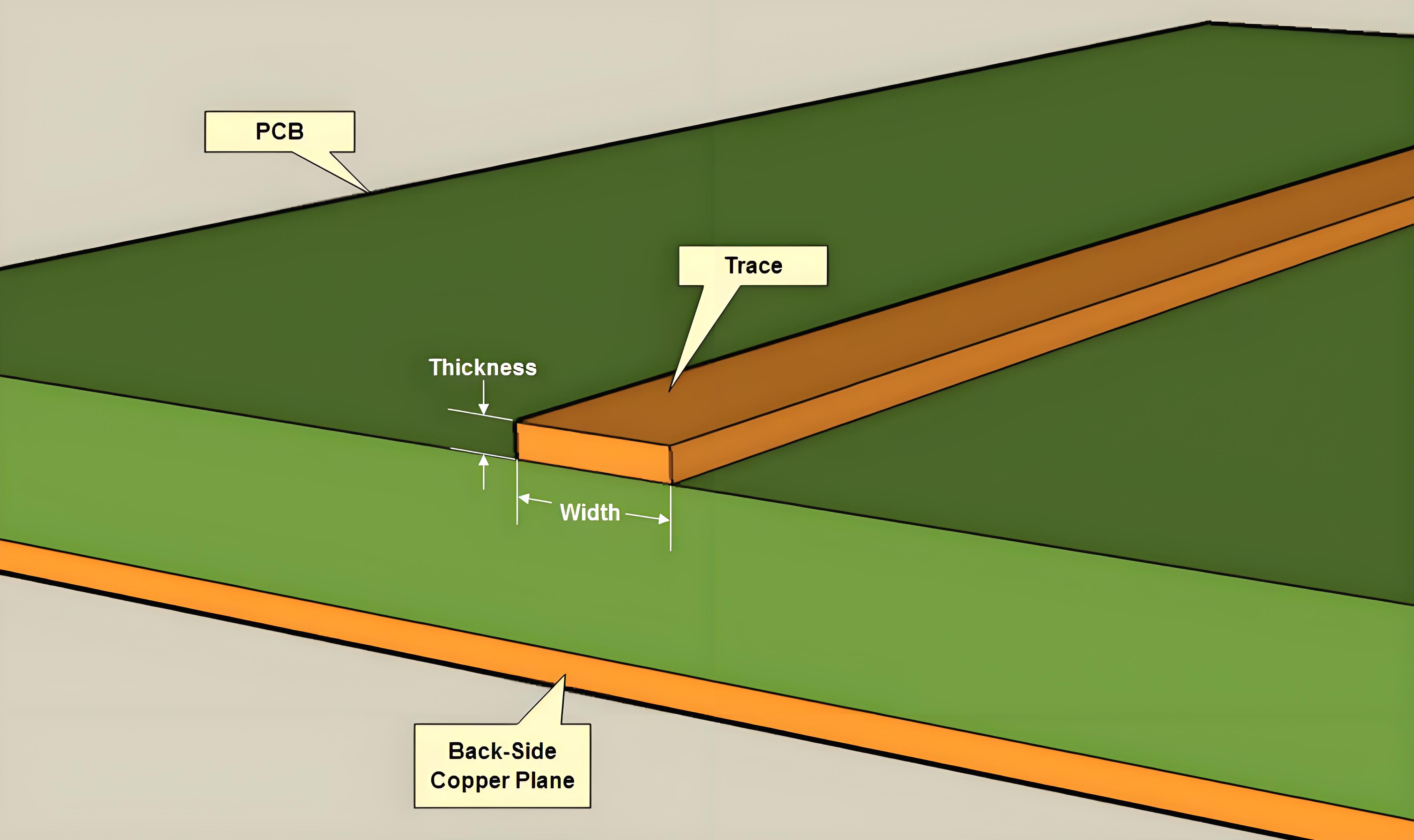
What Is PCB Copper Thickness?
PCB copper thickness refers to the physical dimension of the conductive copper layer applied to a substrate in printed circuit boards. This thickness is typically measured in ounces per square foot (oz), where 1 oz represents approximately 35 micrometers of pure copper deposited uniformly over one square foot area.
It impacts current-carrying capability, heat dissipation, and mechanical resilience of the circuit. Common standardized thicknesses include 0.5 oz for high-frequency signals due to reduced losses, 1 oz for general digital circuits, and 2 oz or higher for power-intensive applications like automotive systems or industrial equipment, where enhanced current handling and thermal management are needed.

PCB Copper Thickness Chart
| Copper Weight (oz) | Thickness (μm) | Max Current (10°C Rise) | Applications | Design Tips |
| 0.5 oz | 17.5 | 0.6A/mm width | HDI, RF, wearables | Use with 0.2-0.3mm traces for signal integrity |
| 1/3 oz (~0.33 oz) | 11.7 | 0.4A/mm width | Ultra-thin flex PCBs | Avoid >0.5A continuous current |
| 1 oz | 35 | 1A/mm width | Standard boards | Default choice for power |
| 2 oz | 70 | 2.3A/mm width | Power supplies | Reduces voltage drop by 50% vs 1oz |
| 15 oz | 525 | 15A/mm width | Heavy power busbars, EV charging | Requires ≥3mm trace width & plating support |
How to Choose PCB Copper Thickness?
1. Calculate Current Capacity First
- Use the IPC-2221 formula: ΔT = (I² * R * t) / (k * A); Where ΔT = temp rise, I = current, R = resistivity, t = trace thickness, k = thermal conductivity, A = cross-sectional area.
- Why: Avoid over-engineering. 1oz (35μm) suits most digital circuits (≤3A), while 2oz+ (70μm+) is required for power traces (>5A).
2. Match Signal Frequency to Copper Thickness
- High-frequency (>1GHz): Use ≤1oz copper to minimize skin effect losses.
- Low-frequency/Power: Opt for ≥2oz copper to reduce I²R losses.
- Why: Balances signal integrity and thermal performance.
3. Factor in Manufacturing Constraints
- Standard PCBs: 0.5oz–4oz (17μm–140μm) is manufacturable.
- Flex/Rigid-Flex: Use ≤1oz copper to prevent cracking during bending.
- Why: Avoid costly redesigns by aligning with fab capabilities.
4. Optimize Cost-Performance Ratio
- 1oz Copper: Cost-effective for 80% of applications (consumer electronics).
- 2oz–3oz Copper: +15–30% cost premium but critical for automotive/industrial.
- Why: Saves 20–40% vs. over-specifying heavy copper.
5. Thermal Management Strategy
- High-Power Zones: Use thick copper (2oz+) or combine with thermal vias.
- Heat Sinks: Embed heavy copper planes (≥3oz) for direct cooling.
- Why: Reduces reliance on external cooling components.
6. Impedance Control Requirements
- Controlled Impedance Traces: Maintain consistent copper thickness (±10% tolerance).
- Why: Ensures signal accuracy in RF/high-speed designs.
How to Measure Copper Thickness on PCB?
Five Methods about how to measure copper thickness on PCB:
Quick Visual Inspection (No Tools)
- Method: Check PCB surface color/texture.
- Thin copper (≤1oz/35μm): Shiny, smooth finish (common in consumer electronics).
- Thick copper (≥2oz/70μm): Matte, rougher texture (visible under angled light).
- Why: Instantly identify gross mismatches (e.g., supplier claims 2oz but delivers 1oz).
Conductive Pen + Multimeter (Low-Cost)
- Tools: Conductive ink pen (20),multimeter(30).
- Steps:
- Draw a 1cm² grid on a scrap PCB section.
- Measure resistance (R) across the grid.
- Use formula: Thickness (μm) = (Resistivity × Width × Length) / (R × Depth).
- (Assume resistivity of copper = 0.01724 Ω·mm²/m).
- Accuracy: ±10% (sufficient for basic QC).
- Why: $50 setup costs, detects 50%+ thickness deviations.
Cross-Section Sampling (Destructive)
- Tools: Razor blade, microscope (smartphone macro lens works).
- Steps:
- Cut a small PCB slice near the edge.
- Polish the cross-section with sandpaper (600→2000 grit).
- Measure copper layer height under microscope.
- Accuracy: ±2μm (if done carefully).
- Why: Confirms supplier claims using $0.50 in tools.
Third-Party Lab Testing (Dispute Resolution)
- Method: Send samples to accredited labs (e.g., SGS, Intertek).
- Tests:
- XRF (50–100/sample) for non-destructive analysis.
- SEM/EDS (200–500) for sub-micron precision.
- Why: Legal-grade evidence for supplier negotiations/lawsuits.
In-Circuit Current Testing (Functional Validation)
- Method:
- Run PCB at max rated current.
- Monitor temperature rise with IR thermometer.
- Compare with thermal models (e.g., ΔT = I²R).
- Failure Sign: Localized hotspots indicate insufficient copper thickness.
- Why: Validates real performance without measuring tools.
Conversion of PCB Copper Weight to Thickness
1. Core Conversion Formula
- Standard Rule: 1 oz/ft² = 1.37 mil (34.79 μm)
2. Adjustments
Post-Etching Thickness Loss:
- Inner layers lose ~10% due to lamination (e.g., 2oz → ~62μm).
- Outer layers lose ~5% after plating/etching.
Surface Finish Impact:
- ENIG adds 0.1–0.15 mil (2.5–3.8 μm) → Compensate in impedance calculations.
3. Advanced Calculation Methods
For Custom Weights:
- Thickness (μm) = Weight (oz/ft²) × 34.79 × (1 – Etching Loss %)
- Example: 3oz with 12% loss → 91.8 μm (vs. theoretical 104.4 μm).
Current-Carrying Capacity:
- Empirical correction for high temps:
- Effective Thickness (μm) = Nominal Thickness × (1 – 0.003 × (T_actual – 25°C))
4. Manufacturing Tolerance Alerts
- IPC-4562 Class B Tolerance: ±10% (e.g., 1oz could be 31.3–38.3 μm).
- Critical Design Tip: Always specify minimum thickness in fab notes (e.g., “2oz, min 60μm post-etch”).
5. Cost vs. Performance Tradeoffs
- Thicker Copper = Higher cost (+40% for 2oz, +120% for 3oz) but enables:
- 2× current capacity (vs. 1oz at same temperature rise).
- 30% lower thermal resistance.
Relationship Between PCB Copper Thickness vs Current
Insufficient Copper Thickness Risks Product Reliability
- Issue: Thin copper layers struggle to handle current, leading to overheating.
- Example: 1oz (35μm) copper carrying 5A → 45°C temperature rise (exceeds safe 30°C limits).
- Benefit: Prevents field failures and costly repairs (up to $200+ per unit).
Over-Specified Copper Wastes Budget
- Challenge: Unnecessarily thick copper increases costs by 15–40%.
| Application | Recommended Thickness | Cost vs 1oz (35μm) |
| Low-Power (<3A) | 1oz | Base cost |
| Industrial (5A) | 2oz | +18% |
| High-Power (10A) | 3oz | +35% |
- Benefit: Optimizes cost by matching thickness to actual current needs.
IPC-2221 Formula: Data-Driven Calculation
- Formula: I = k × (ΔT)^0.44 × (A)^0.725
- I = Current (A)
- k = 0.048 (external traces), 0.024 (internal traces)
- ΔT = Allowable temperature rise (keep ≤30°C)
- A = Cross-sectional area (mm²) = Thickness (μm) × Trace Width (mm) / 1000
- Benefit: Quickly calculate minimum copper thickness (e.g., 5A/5mm trace → 2oz required); Avoids under-engineering (risks) or over-engineering (costs).
Supplier Accuracy: Verify Thickness Claims
- Risk: Some manufacturers use thinner “rolled copper” than advertised.
- Solutions: Low-Cost Validation: Use a conductive pen + multimeter (formula: Thickness (μm) = 0.01724 × Trace Width (mm) / (Resistance × Trace Length (mm))).
- High-Precision Validation: Third-party XRF testing (50–100/sample).
- Benefit: Ensures labeled thickness matches reality, avoiding hidden quality issues.
Client Action Checklist
- Design Phase: Use IPC formula to calculate thickness + 20% safety buffer.
- Procurement: Specify tolerance in contracts (e.g., “2oz ±0.2oz”).
- Incoming Inspection: Randomly test 1% of batches with conductive pen.
- Dispute Resolution: Present third-party reports to enforce warranties.
PCB Copper Thickness Calculator
| Tool | Features | Best For |
| Saturn PCB Toolkit | • IPC-2152 compliant • Auto-derating • Impedance modeling | Power electronics |
| EEWeb Online Calculator | • Temperature rise graphs • Exportable reports • Mobile-friendly | Quick field checks |
| Altium Integrated Tool | • Real-time DRC • Multi-layer analysis • 3D thermal simulation | Altium users |
Welcome to contact EBest Circuit (Best Technology) if you need to calculate PCB copper thickness: sales@bestpcbs.com.