

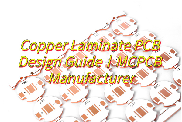
Looking for copper laminate PCB solution? This blog discover its material, specification, benefits, applications, design guide for LED lighting, manufacturing process.
Are you worried about these problems?
- Uneven heat dissipation leads to a dramatic reduction in component lifespan. How can we overcome thermal management challenges?
- High-frequency signal integrity is insufficient. How can we balance electromagnetic compatibility and transmission efficiency?
- Low-volume customization leads to long lead times. How can we balance flexibility and cost control?
EBest Circuit (Best Technology) can provide solutions include:
- Gradient heat dissipation structure design: Through optimized three-dimensional heat conduction paths, it achieves a temperature drop of over 15°C in hotspots, extending device lifespan.
- Low-impedance electromagnetic shielding layer: Utilizing high-purity aluminum-based nano-plating technology, signal transmission loss is reduced to 0.3dB/cm.
- Agile and flexible production lines: Prototyping within 48 hours, supporting minimum orders of 10 pieces, and reducing mass production cycle time by 30%.
Welcome to contact us if you have any request for metal core PCB: sales@bestpcbs.com.
What Is Copper Laminate PCB?
A Copper Laminate PCB is a printed circuit board base material that consists of an insulating substrate (such as FR4, CEM-1, ceramic, or metal core) that is laminated with a thin layer of copper foil on one or both sides. This copper layer is later etched to create electrical pathways or circuit traces, which connect and support electronic components.
What Is Material of Copper Clad PCB?
Materials of Copper Clad Laminate (CCL) PCB
Base Substrate Materials:
- Epoxy Resin (FR-4): Most common, combining glass fiber cloth with epoxy for rigidity and insulation.
- Polyimide (PI): Used in flexible PCBs for high-temperature resistance and bendability.
- Phenolic Resin: Low-cost option for paper-based CCLs, suited for simple circuits.
- PTFE (Teflon): High-frequency applications due to ultra-low dielectric loss.
Reinforcement Materials:
- Glass Fiber Cloth (E-glass): Primary reinforcement in rigid CCLs for strength and stability.
- Paper/Cellulose: Used in cost-sensitive, low-performance boards.
- Polyester/PET Film: Base for flexible CCLs in lightweight designs.
Conductive Layer
- Electrolytic Copper Foil: Purity ≥99.8%, thickness ranges from 18μm (0.5oz) to 105μm (3oz).
- Rolled Copper Foil: Smoother surface for high-frequency signals.
Specialty Materials
- Metal-Core (Aluminum/Copper): For high-power LED and automotive PCBs, offering superior heat dissipation.
- Ceramic-Based: High thermal conductivity for RF/microwave circuits.
Adhesive Systems
- Modified Epoxy: Bonds copper foil to substrates, ensuring peel strength ≥1.0N/mm.
- Acrylic/Polyimide Adhesives: Used in flexible CCLs for dynamic bending applications.
Copper Clad Laminate PCB Specification
| Parameter | Standard Values |
| Base Material | Metal-Core (Cu) |
| Copper Foil Thickness | 18μm–105μm (0.5oz–3oz) |
| Dielectric Constant (Dk) | 3.8–4.5 (FR-4), 2.5–3.5 (PTFE) |
| Dissipation Factor (Df) | 0.015–0.025 (FR-4), <0.005 (PTFE) |
| Thermal Conductivity | 150–400 W/m·K (Metal-Core) |
| Peel Strength | ≥1.0 N/mm (Cu-to-substrate) |
| TG Rating | Tg 130°C–170°C (Standard/High-Tg) |
| Flammability Rating | UL94 V-0 (Halogen-free options) |
What Are Benefits of PCB Copper Clad Laminate?
- Enhanced Signal Integrity: Lowers ground impedance, reducing noise and interference in digital circuits (e.g., pulse current paths are optimized).
- Improved Heat Dissipation: Copper’s high thermal conductivity (≈400 W/m·K) helps distribute heat evenly, preventing hot spots.
- Mechanical Stability: Reinforces PCB structural integrity during manufacturing, reducing warping and deformation.
- EMI/RFI Shielding: Acts as a natural shield against electromagnetic interference, protecting sensitive components.
- Design Flexibility: Supports high-density interconnects (HDI) and advanced techniques like blind/buried vias for compact electronics.
- Cost-Effective Manufacturing: Simplifies processes (e.g., plating-filled vias for reliable connections) while maintaining performance.
What Are Applications of Copper Laminate PCB?
- Telecommunications: 5G base stations, RF signal processing modules.
- Automotive: Electric vehicle (EV) battery management systems, motor control units.
- Lighting: High-power LED drivers, automotive headlight assemblies.
- Aerospace: Satellite communication hardware, avionics control systems.
- Consumer Electronics: Smartphone motherboards, IoT device circuitry.
- Medical: MRI machine power supplies, implantable medical device interfaces.
- Industrial Automation: Robotics motor drivers, factory automation control panels.
- Renewable Energy: Solar inverter power conversion, wind turbine energy management systems.
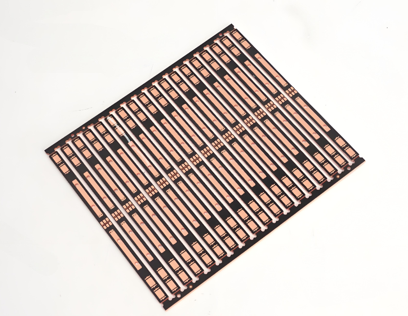
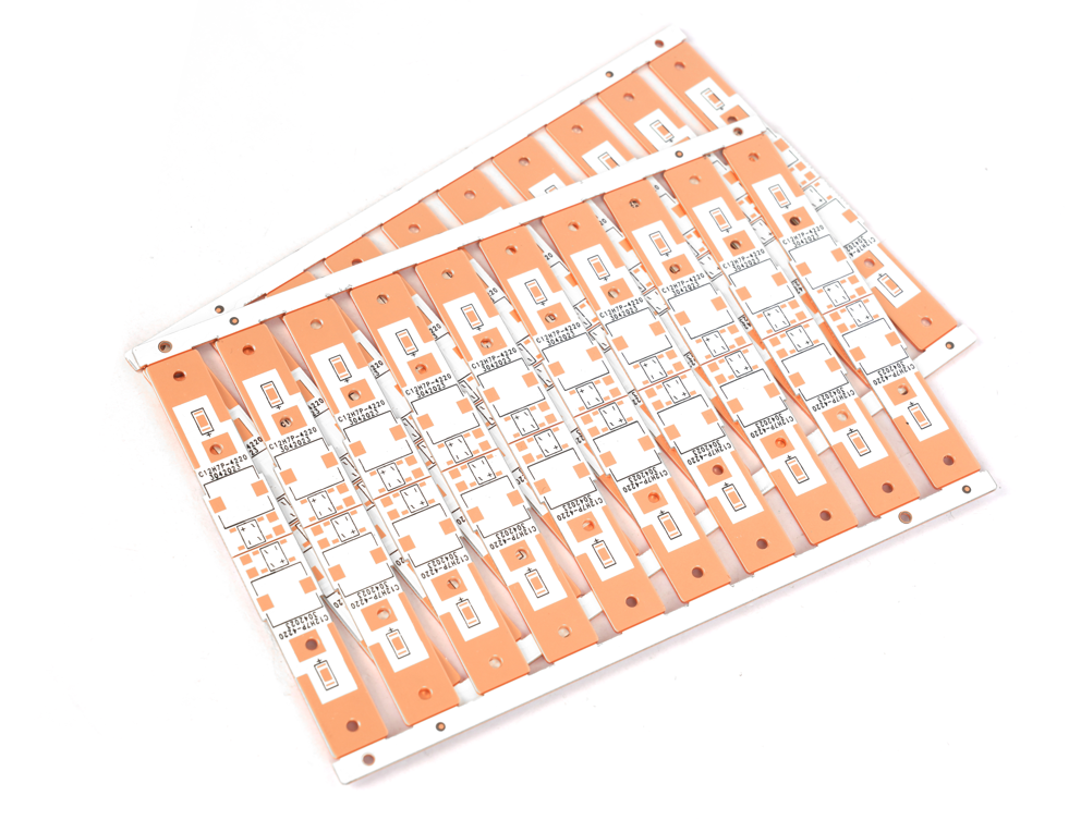
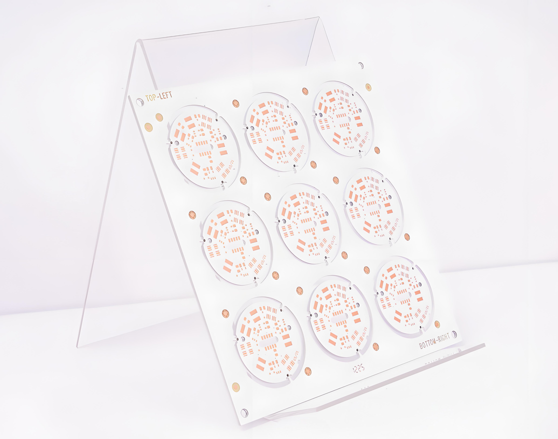
Copper Laminate PCB Design Guide For LED Lighting
Below are copper laminate PCB design guide for LED lighting:
1. Material Selection
- Base Material: Use electrolytic copper foil (ED Copper) with minimum thickness 1 oz (35µm).
- Dielectric Layer: Select UL94 V-0 certified insulation (e.g., polyimide or ceramic-filled epoxy).
- Copper Purity: ≥99.9% purity for thermal/electrical performance. Surface roughness (Ra) ≤1.6µm.
2. Layer Stackup
- Single-Layer: Copper substrate (bottom) + dielectric + copper trace layer (top).
- Multi-Layer: Avoid placing signal layers directly on copper substrate. Use “copper substrate – dielectric – copper foil” for dual layers.
- Prohibition: No signal traces on copper substrate side.
3. Trace Routing
- Current Capacity: Follow IPC-2221. Design traces ≥3mm/A for high-current paths (e.g., LED drivers).
- Clearance: Maintain ≥2mm spacing between traces and copper substrate edges.
- Geometry: Use 45° miters for bends; avoid 90° angles.
4. Thermal Management
- Thermal Vias: Place via arrays (≥0.3mm diameter, ≤1mm pitch) under high-power LEDs. Connect directly to copper substrate.
- Solder Mask: Exclude solder mask on copper substrate areas for direct thermal dissipation.
- Copper Coverage: Allocate ≥40% of PCB area to copper substrate for heat spreading.
5. Solder Mask
- Thickness: Control solder mask on copper substrate to 15–25µm.
- Clearance: Keep solder mask openings ≥0.5mm from copper substrate edges.
- Process: Avoid LPI (Liquid Photoimageable) solder mask on copper substrate side.
6. Via Design
- Drilling: Mechanical vias ≥0.8mm; laser vias ≥0.15mm.
- Teardrops: Add teardrop reliefs at via-to-trace junctions.
- Grounding: Minimum 2 vias per high-power LED for thermal/ground connectivity.
7. Test Points
- Placement: Locate test pads away from copper substrate areas.
- Size: Test pad diameter ≥2mm; spacing ≥2.54mm.
- Accessibility: Ensure test points are probe-friendly (no components nearby).
8. Manufacturing Tolerances
- Outline: Board dimension tolerance ±0.1mm.
- V-Cut: Depth ≤1/3 of total board thickness.
- NPTH: Avoid non-plated through-holes (NPTH) near copper substrate.
9. Reliability Testing
- Thermal Cycling: -40°C to +125°C, 1000 cycles.
- Humidity: 85°C/85%RH for 500 hours.
- Solderability: 260°C/10s reflow, 3 cycles.
10. Documentation
- Annotations: Specify copper thickness, dielectric material, and thermal via locations.
- Thermal Model: Provide 3D thermal simulation files (e.g., Ansys Icepak).
- Assembly Notes: Highlight LED polarity, thermal pad alignment, and pressure requirements.
Single Sided Copper Clad Laminate PCB Manufacturing Processes
Single-Sided Copper Clad Laminate PCB Manufacturing Processes
1. Material Preparation
- Use FR-4 or CEM-1 substrate with 1 oz (35µm) electrolytic copper clad on one side.
- Cut raw panels to working size (e.g., 400mm × 500mm) with ±1mm tolerance. Clean edges to remove debris.
2. Drilling
- CNC drill component/mounting holes using carbide bits (0.3mm–3.2mm diameter).
- Deburr holes with nylon brush or ultrasonic cleaner. Inspect for broken bits or residual copper.
3. Surface Cleaning
- Alkaline wash (pH 10–12) to remove oils and fingerprints.
- Micro-etch copper surface with sulfuric acid + hydrogen peroxide solution (Ra 1.6–3.2µm).
- Dry at 80–100°C to prevent oxidation.
4. Circuit Formation
- Apply dry film photosensitive laminate (35–50µm) or screen-print etch-resistant ink.
- Expose to UV light through artwork film (1–5 seconds). Develop with sodium carbonate (0.8–1.2% concentration).
5. Etching
- Use ferric chloride (FeCl₃) solution at 45–55°C or ammonium persulfate at 25–30°C.
- Spray etch with 1.5–2.5 kg/cm² pressure for uniformity. Control line width (±10% tolerance) and undercut (<10% of line width).
- Rinse with water and strip residual dry film with sodium hydroxide (2–3% solution).
6. Solder Mask Application
- Spray or screen-print epoxy-based liquid photoimageable (LPI) solder mask (20–30µm thickness).
- Expose to UV through solder mask film. Develop with sodium carbonate (1–2% concentration). Cure at 150°C for 60 minutes.
7. Surface Finish
- HASL: Dip in molten Sn63/Pb37 solder (260°C) and blow hot air to remove excess.
- OSP: Apply benzotriazole-based coating. Dry at 80°C for 10–15 minutes.
8. Profiling
- Score board edges with V-Cut (30–60° angle) using hydraulic press. Maintain ±0.1mm dimensional tolerance.
9. Electrical Testing
- Use flying probe tester (e.g., Takaya APT-9411) with 10–50V DC. Verify isolation resistance (>100MΩ) and continuity (<1Ω).
10. Quality Inspection
- Visual check: No exposed copper outside solder mask, no voids/cracks, pad alignment ±0.05mm tolerance.
- Dimensional check: Hole positions (±0.1mm), board size (±0.2mm).
11. Packaging
- Vacuum seal boards in ESD-safe bags with desiccant. Label with lot number, date code, and RoHS compliance mark.
Why Choose EBest Circuit (Best Technology) as MCPCB Manufacturer?
- 19-Year Metal Substrate Expertise: Avoid costly design iterations with battle-tested thermal management solutions.
- Strict Quality Control: 100% AOI/X-ray inspection ensures flawless delivery, eliminating rework risks.
- 24-Hour Rapid Prototyping: Cut product validation time by 50% and accelerate market entry.
- ISO 9001/14001 Certified: Global regulatory compliance simplified for seamless international sales.
- Competitive Pricing: Achieve 20%+ cost savings through optimized production scaling.
- Custom Thermal Management: Optimize heat dissipation for high-power applications (e.g., automotive, LED).
- Flexible MOQ (5pcs–100K+): Reduce inventory risks with agile small-batch to mass-production transitions.
- 24/7 Engineering Support: Solve technical challenges proactively, shorten R&D cycles by 30%.
Welcome to contact us if you have any inquiry for metal core PCB: sales@bestpcbs.com.