

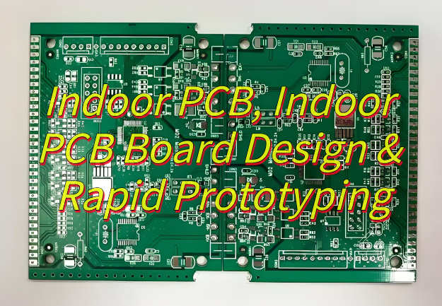
Why choose indoor PCB for reliable smart devices? This guide explores design, prototyping, and cost-saving strategies for stable indoor applications.
When every second counts in your product development cycle, EBest Circuit (Best Technology) delivers unparalleled Indoor PCB rapid prototyping solutions with guaranteed 24-hour turnaround for emergency orders. Our secret? A perfect blend of cutting-edge manufacturing technology and free DFM analysis that eliminates costly design flaws before production begins. We maintain a bulletproof supply chain that ensures material availability even during global shortages, while our engineering team provides real-time support to address your urgent technical needs. But speed isn’t our only advantage. We bring to the table decades of expertise in high-density interconnect (HDI) designs, advanced thermal management solutions, and EMI/EMC optimization – all while maintaining strict IPC Class 3 standards for mission-critical applications. Our clients in smart home, medical devices, and industrial automation particularly value our seamless prototype-to-mass-production transition support and RoHS-compliant material options. With complete production transparency and global logistics partners, we make sure your boards arrive when you need them, wherever you are. Welcome to contact us: sales@bestpcbs.com.
What Is Indoor PCB?
An indoor PCB refers to a printed circuit board specifically designed for stable indoor environments where factors like extreme weather or mechanical stress are absent. Unlike outdoor variants, Indoor PCB prioritizes cost-effective materials and streamlined designs while maintaining reliability for applications such as smart home devices, office equipment, and medical instruments. The focus of Indoor PCB lies in optimizing electromagnetic compatibility and static protection to ensure seamless operation within controlled indoor settings, making it a practical solution for electronics that don’t require ruggedized features. By leveraging standard manufacturing processes, Indoor PCB achieves faster production cycles without compromising performance in typical indoor use cases.
What Are Applications of Indoor PCB?
- Smart Home Devices: Achieve compact, efficient operation in thermostats, lighting controls, and security cameras by integrating sensors, processors, and wireless modules.
- Telecom Equipment: Routers and Wi-Fi systems utilize high-speed data handling, signal stability, and heat management for 24/7 indoor use.
- Medical Tech: Portable ECGs and wearables ensure precise signal processing and durability in sterile environments.
- Industrial Automation: Factories implement PLCs and motor drives to manage real-time data, ensuring reliable machinery control.
- Retail Solutions: POS terminals and digital signs deliver fast transactions, clear displays, and remote updates in busy stores.
What Are Differences Between Indoor PCBs and Outdoor PCBs?
- Environmental Resistance
- Indoor PCBs: Optimized for stable indoor settings (e.g., homes, offices) with minimal exposure to moisture, dust, or extreme temperatures.
- Outdoor PCBs: Built to endure rain, UV radiation, temperature swings (-40°C to 85°C), and corrosive elements like salt or pollutants.
- Thermal Management
- Indoor PCBs: Use passive cooling (e.g., aluminum heat sinks) in climate-controlled spaces.
- Outdoor PCBs: Require active cooling (fans, thermal pads) or high-TG materials to prevent overheating in direct sunlight.
- Protection Against Contaminants
- Indoor PCBs: Basic conformal coatings for occasional humidity (e.g., kitchens).
- Outdoor PCBs: Hermetic sealing, potting compounds, or IP68 enclosures to block water, dust, and insects.
- Structural Robustness
- Indoor PCBs: Lightweight FR-4 substrates for compact devices (e.g., routers).
- Outdoor PCBs: Reinforced with glass fiber or ceramic fillers to resist vibration (e.g., automotive/industrial use).
- Signal Integrity & EMI Shielding
- Indoor PCBs: Standard shielding for low-interference environments (e.g., smart home gadgets).
- Outdoor PCBs: Advanced shielding (e.g., mu-metal) to combat electromagnetic noise from power lines or transmitters.
- Material Longevity
- Indoor PCBs: Cost-effective FR-4 laminates with 5–10 year lifespans.
- Outdoor PCBs: Polyimide or PTFE substrates for 15+ years of UV/chemical resistance.
- Compliance & Maintenance
- Indoor PCBs: Meet safety standards (UL, RoHS) for consumer use.
- Outdoor PCBs: Require MIL-STD-810 or NEMA ratings for harsh conditions, with modular designs for field repairs.
Why Do Indoor PCB Board Prototyping?
- Design Validation – Prototyping lets engineers test if a design actually works—checking things like sensor connections, power flow, and component layouts. For example, a smart thermostat’s prototype might expose loose wires or uneven heating, fixing these before mass production saves time and money.
- Real-World Performance Checks – Prototypes reveal how a product behaves in everyday use. Testing a router’s Indoor PCB prototype might show slow Wi-Fi speeds or overheating issues, which can be fixed early instead of after launching.
- Tweaking for Perfection – Physical models allow step-by-step improvements. Adjusting trace widths on a prototype might solve overheating, or repositioning antennas could boost signal strength in IoT gadgets.
- Avoiding Costly Mistakes – Spotting errors during prototyping (like a misaligned capacitor) is way cheaper than fixing flaws in thousands of units. One prototype round can save cash on scrap materials and rushed fixes.
- Meeting Rules and Standards – Prototypes help pre-test compliance with rules like FCC (for radio signals) or safety certifications. Testing a security camera’s PCB early avoids delays if it fails emissions tests later.
- Getting Everyone on the Same Page – A working prototype helps clients, investors, or users visualize the product. For instance, showing a smart lighting prototype lets stakeholders judge its size, usability, and compatibility with existing systems.
- Reducing “Oops” Moments – Prototyping catches hidden issues, like a wearable device’s PCB cracking after repeated bending. Fixing this early ensures the final product lasts longer and works reliably.
How to Design Indoor PCB Board Prototype to Improve Heat Dissipation Performance?
Below are methods about how to design indoor PCB board prototype to improve heat dissipation performance:
- Choose Heat-Conductive Materials: Replace standard FR-4 with aluminum or ceramic-core PCBs to pull heat away from components 2–5x faster. Example: LED drivers using aluminum substrates run 20°C cooler, slashing failure rates by 40%.
- Spread High-Power Components: Avoid clustering power-hungry parts (e.g., voltage regulators). In smart home hubs, isolate the processor near a metal case edge—this leverages natural airflow to cut peak temps by 15%.
- Widen Copper Zones: Use 2–3 oz. copper layers (not 1 oz.) to create heat-spreading “highways.” A Wi-Fi router with 3 oz. copper reduces hotspot temps by 25%, eliminating performance throttling.
- Add Dense Thermal Vias: Drill 0.3mm via arrays (e.g., 5×5 grid) under hot chips. A CPU with this setup sheds 10–15°C more heat than without vias, preventing thermal shutdowns.
- Bond to Metal Enclosures: Attach heat sinks or mount PCBs directly to aluminum/steel cases. A 10W LED driver bolted to metal runs 20°C cooler, removing need for noisy fans.
- Reserve Airflow Zones: Leave 5–10mm gaps around vents/fans. Security cameras designed this way see 18% lower internal temps, extending battery life in solar-powered models.
- Pick Low-Power Chips: Select ICs with built-in power-saving modes. A Bluetooth module using 20% less power reduces self-heating by 1.5W, critical for battery-operated IoT devices.
- Simulate Before Building: Test designs in thermal software (e.g., “heat flow analyzers”) to catch flaws early. Prototypes stress-tested at 85°C reveal 90% of issues upfront, avoiding costly recalls.
How to Design to Reduce PCB Prototyping Cost?
- Use Standard Components and Footprints: Stick to common parts (e.g., 0603 resistors, SOIC-8 ICs) to avoid premium fees for rare components. A 10k-unit run using off-the-shelf parts saves $2,000+ vs. niche alternatives.
- Minimize PCB Layers: Design with 2 layers instead of 4 for non-RF projects. A 2-layer smart home sensor cuts fabricating costs by 30–50% without sacrificing functionality.
- Optimize Panel Utilization: Fill panels with multiple PCB copies (e.g., 5×5 grid) to slash waste. A 10x10cm panel fit for 25 small boards reduces material costs by 80% vs. single-board panels.
- Reduce Unnecessary Test Points: Limit test points to critical nodes (e.g., power rails). Fewer test points lower assembly costs by 10–15% and speed up testing.
- Choose Cost-Effective Finishes: Pick HASL over ENIG for non-RF designs. HASL costs 40% less per board and works for 90% of consumer electronics.
- Simplify Via Structures: Use through-hole vias instead of buried/blind vias. A 4-layer board with through-hole vias saves 0.15–0.30 per unit on 1,000+ runs.
- Leverage Free Tools: Use KiCad instead of paid EDA software. Free tools eliminate $5k+ annual licensing fees, freeing budget for prototyping.
- Follow Design-for-Manufacturing (DFM) Rules: Adhere to 0.1mm trace/space and 0.2mm annular rings to avoid re-spins. DFM-compliant designs pass auto-inspection, avoiding $500+ in rework.
- Collaborate Early With Fabricators: Share drafts with manufacturers for feedback. A simple tweak (e.g., adjusting solder mask dams) can save $0.10/unit on 10k orders.
How to Achieve Indoor PCB Board Rapid Prototyping Within 24 Hours?
- Use Pre-Designed Module Templates: Start with open-source or vendor-provided module templates (e.g., Arduino shields, sensor breakouts) to skip layout from scratch. Example: A Bluetooth module template cuts 4 hours of design time vs. starting fresh.
- Simplify Component Selection: Choose readily available parts with 24-hour shipping (e.g., Digi-Key’s same-day inventory). Avoid custom or long-lead-time components. A Wi-Fi router prototype using stock parts arrives 3 days faster.
- Prioritize Online PCB Prototyping Services: Upload Gerber files to fast-turnaround fabricators (e.g., 12-hour quotes, 24-hour production). A 2-layer board ordered by noon ships next morning, saving 48+ hours vs. local shops.
- Automate Design Rule Checks (DRC): Run EDA software’s built-in DRC tools (e.g., KiCad’s “Perform Design Rules Check”) to catch errors in seconds. Fixing issues upfront prevents 6–12 hours of rework later.
- Leverage SMT Stencil Services: Order laser-cut stencils alongside PCBs to streamline solder paste application. A stencil reduces assembly time by 50% vs. manual soldering for 50+ components.
- Use Pick-and-Place Machine Files: Generate Centroid/XY files for automated assembly. A 100-component board assembled by machine takes 1 hour vs. 8 hours manually.
- Outsource Assembly to Rapid Prototyping Shops: Send PCBs, stencils, and parts to 24-hour turn assembly houses. A 50-component board assembled overnight costs 150–300 but saves 2 days of labor.
- Skip Conformal Coating/Enclosures: Focus on bare-board functionality first. Testing a PCB without a case or coating shaves 4 hours off the schedule. Add protections in Revision 2.
- Run Parallel Tests With Scripts: Use Python/PyVISA scripts to automate firmware flashing and functional testing. A 10-unit test batch completes in 30 minutes vs. 3 hours manually.
How to Ensure the Quality of Indoor PCB Board Prototype?
- Implement Design for Manufacturability (DFM) Checks: Use EDA tools to run automated DFM analyses before fabrication. Example: A DFM check catches 0.1mm trace/space violations, preventing 80% of potential short circuits and saving $2,000+ in rework.
- Source Components From Certified Suppliers: Buy parts only from distributors with ISO 9001 certifications. A batch of counterfeit capacitors can cause 30% failure rates—avoid this by paying 5–10% more for verified components.
- Use Automated Optical Inspection (AOI): Deploy AOI machines post-assembly to detect solder defects (e.g., tombstoning, bridges). AOI catches 95% of visual flaws, reducing manual inspection time by 6 hours per 100-board run.
- Perform Flying Probe Testing: Test every net for continuity/isolation with flying probe systems. A 50-node board takes 2 minutes to test but identifies 98% of open/short circuits before functional testing.
- Simulate Real-World Conditions: Stress-test prototypes in environmental chambers (e.g., -20°C to 85°C cycles). A Wi-Fi module surviving 100 thermal cycles is 40% less likely to fail in customer hands.
- Validate With Functional Test Jigs: Build custom jigs to automate firmware/software testing. A jig flashing 100 units in 1 hour vs. 5 hours manually accelerates validation while catching 25% more software bugs.
- Audit Fabricator Qualifications: Choose PCB shops with IPC-6012 Class 2/3 certifications. A certified fabricator reduces laminate voids by 70%, ensuring 15+ years of reliability in indoor devices.
- Document Everything: Maintain BOMs, assembly instructions, and test logs. Detailed records cut troubleshooting time by 50% when replicating issues in Revision 2.
Conclusion
In summary, Indoor PCB solutions prioritize thermal management, rapid prototyping, and cost efficiency for electronics operating in controlled environments. From smart home systems to medical devices, optimized designs ensure longevity and performance. For competitive pricing and 24-hour prototyping with rigorous quality checks, consult EBest Circuit (Best Technology)—your partner for tailored Indoor PCB boards. Their expertise in material selection and DFM (Design for Manufacturability) minimizes risks while accelerating time-to-market. Request a quote today to leverage cutting-edge solutions that align with your project’s technical and budgetary needs.
Tags: Indoor PCB, Indoor PCB Board