

Why is embedded PCB design the future of compact electronics? This guide covers aspects from design tools to thermal optimization and non-destructive testing.
EBest Circuit (Best Technology) sets the industry benchmark for rapid embedded PCB manufacturing by consistently delivering complex designs 40% faster than competitors without compromising IPC Class 3 standards. Our proprietary “Speed-Stack” manufacturing system integrates AI-driven design validation, in-house laser micromachining, and pre-tested component libraries to slash typical 6-week lead times to just 10 business days. With 24/7 manned production lines and drone-assisted logistics, we’ve achieved a 99.8% on-time delivery rate for over 2,300 embedded PCB projects in 2024, including mission-critical medical and aerospace applications. Clients benefit from our real-time production tracking portal and guaranteed 72-hour prototype turnaround– a capability validated by three patents in accelerated multilayer bonding and high-speed impedance testing. Welcome to contact us: sales@bestpcbs.com.
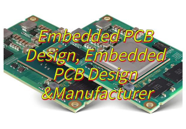
What Is Meant by Embedded PCB Design?
Embedded PCB design refers to the process of integrating electronic components directly into the layers of a printed circuit board (PCB). This approach allows for a more compact, efficient, and reliable electronic system. Instead of having components mounted on the surface or through holes of the PCB, they are embedded within the board’s structure. With embedded PCB design, you can achieve better electrical performance, reduce electromagnetic interference, and enhance the overall durability of the PCB. This type of design is becoming increasingly popular in various industries, from consumer electronics to aerospace, as it enables the creation of smaller, faster, and more power-efficient devices. Embedded PCB design is not just about placing components; it involves careful planning and engineering to ensure that all elements work harmoniously together within the confined space of the PCB.
How to Choose Embedded PCB Design Tools?
- Functionality: Choose tools that support component embedding, high-speed signal processing of multilayer boards, and impedance matching calculations. For example, Altium Designer’s Component Placement Editor can achieve precise embedding, and PADS Professional’s interactive routing can handle complex topologies. At the same time, ensure that the tool has SPICE-level circuit simulation capabilities to verify power integrity and signal quality in advance.
- User Interface: Give priority to tools that can customize shortcut keys and workspace layouts, such as KiCad, which supports users to save personalized interface configurations. It is recommended to use a router with real-time preview function, such as Eagle’s automatic push routing, which can intuitively see the routing effect and reduce rework.
- Compatibility: Confirm that the tool supports mainstream format conversion, such as Gerber RS-274X output and STEP 3D model import. Design tools integrated with common version control tools (such as Git) can achieve file version traceability during team collaboration. Avoid using tools that only support proprietary formats to prevent data migration difficulties.
- Scalability: When dealing with high-density designs with more than 5,000 components and more than 20 layers, the tool should be able to run smoothly on an ordinary workstation (more than 16GB of memory). It is recommended to choose tools that support distributed computing, such as Cadence Allegro, which can use multi-core CPUs to accelerate DRC checks and avoid lags in large projects.
- Support and Updates: Choose vendors that provide quarterly security patches and feature updates, such as Mentor Graphics, which releases 2-3 major version updates per year. Make sure the vendor provides a 24-hour technical support channel that can quickly respond to DRC errors, library file compatibility and other issues through online work orders, phone calls, etc.
- Cost-effectiveness: Startup teams can consider open source tools (such as KiCad) or subscription services (such as Altium Designer, which is paid monthly) to avoid high one-time investments. When comparing tools, focus on calculating the usage rate of functions. For example, if only basic routing functions are used each month, expensive full-featured kits will be wasted.
- Community and Resources: Choose tools with active code maintenance on GitHub and dedicated sections on Stack Exchange. For example, the Easy EDA community updates 10+ practical cases every day, and its official knowledge base contains complete tutorials from entry to high-speed design, making it easy for designers to quickly solve common problems.

What Is the Design Process for Embedded PCB?
Below are design processes for Embedded PCB:
- Requirements gathering: The first task is to clarify the requirements of the embedded printed circuit board (PCB). This requires not only a deep understanding of the electrical parameters of the final product, such as operating voltage, current, signal frequency, etc., but also mechanical constraints, such as PCB size, shape, mounting hole location, etc., as well as clear performance expectations, such as processing speed and stability requirements. Accurately grasping the functional goals of the PCB is the cornerstone of ensuring the success of embedded PCB design.
- Component selection: When selecting suitable electronic components for embedded design, many factors need to be considered comprehensively. The physical size of the component must fit the compact PCB space layout; the power consumption index must meet the device endurance and heat dissipation requirements; the functional characteristics must accurately match the design requirements. In addition, the selected components should also be compatible with the embedding process to ensure that they can meet the overall design standards of the embedded PCB.
- Schematic design: Draw a detailed circuit schematic to clearly present the electrical connection relationship between all components. This link is a key step to ensure the normal operation of the embedded PCB function. A well-designed schematic, like a construction blueprint for subsequent layout design, lays a solid foundation for the entire design process.
- Layout planning: When planning the layout of an embedded PCB, you need to consider all factors such as component placement, wiring channels, and power distribution. Reasonable optimization of the layout can effectively reduce mutual interference between signals on the one hand, and ensure efficient heat dissipation on the other hand. Excellent layout planning is the core of achieving high-performance embedded PCBs.
- Component embedding: According to the design plan, the selected components are accurately integrated into each layer of the PCB. This process relies on high-precision manufacturing processes to ensure that the components are firmly embedded and reliable electrical connections are achieved. The quality of component embedding will directly affect the operational reliability of the embedded PCB.
- Routing: The electrical circuits are laid out on the PCB to connect various components. Advanced routing algorithms and technologies are used to optimize the circuits to ensure signal integrity and power transmission efficiency. As a key link in embedded PCB design, routing has a significant impact on the overall performance of the PCB.
- Design rule checking (DRC): Perform design rule checking to verify whether the design strictly follows all design specifications and manufacturing requirements. Through DRC, potential problems can be discovered and corrected in time before the PCB goes into production, which is an indispensable quality control method in embedded PCB design.
- Electrical simulation: Conduct electrical performance simulation analysis to explore the operating performance of embedded PCB under different working conditions. With the help of simulation, the actual working state of the PCB can be predicted in advance, and the optimization points can be accurately located, providing a strong basis for design improvement.
- Mechanical design considerations: Incorporate mechanical design elements into the overall plan, including determining the thickness of the circuit board, planning the location of the mounting holes, and selecting suitable connectors. Ensure that the mechanical design is perfectly matched with the overall system requirements to ensure the installation and use of the PCB in actual applications.
- Design review: Conduct a comprehensive design review with other engineers or project stakeholders. Through multi-party communication and review, problems that may be overlooked in the design can be discovered, and potential optimization suggestions can be put forward to further improve the embedded PCB design.
How to Optimize the Heat Dissipation Design of Embedded PCB?
Component Placement:
- Prioritize the placement of chips with high heat generation (such as CPU, power amplifier) at the edge or corner of the PCB, away from temperature-sensitive components (such as crystal oscillators, sensors), with a spacing of at least 5mm.
- For vertically mounted PCBs, the heat generating components should be placed at the top to dissipate heat naturally by utilizing the principle of rising hot air; when installed horizontally, the layout should be combined with the direction of the chassis air duct to ensure that the arrangement direction of the components is consistent with the direction of the airflow.
Thermal vias:
- Use vias with a diameter of 0.3-0.5mm, and place 8-16 vias in an array form (recommended spacing ≤1mm) under the power device to ensure that the heat conduction path between each layer of PCB is unobstructed.
- For the inner power/ground layer of the multi-layer board, the inter-layer thermal coupling efficiency is enhanced by quincunx-shaped or grid-shaped via layout.
Thermal Interface Materials:
- For BGA packaged chips, it is recommended to use silicone grease with a thermal conductivity of ≥3W/mK, and the coating thickness is controlled at 0.1-0.2mm to ensure that the bottom of the chip is completely covered.
- Install a thermal conductive silicone pad between the radiator and the PCB. Select a material with a Shore hardness of 40-60 according to the pressure requirements to effectively fill the tiny gap.
Copper Plane Design:
- Lay a complete solid copper foil in the power module and processor area. The copper foil thickness is recommended to be 2oz (70μm) or more. The heat dissipation capacity is improved by increasing the copper cladding area.
- For high-frequency signal areas, a grid-shaped copper cladding design is adopted, and the grid width is ≥0.3mm to avoid affecting the signal integrity.
Ventilation Holes:
- Open circular ventilation holes with a diameter of 1-3mm in the concentrated heat generation area of the PCB, and the hole spacing is maintained at 5-10mm to form a honeycomb array structure.
- The ventilation hole layout needs to avoid the signal line, power line and pad area, and the mechanical strength is enhanced by adding a teardrop structure.
Component Selection:
- Give priority to low-power devices, such as using TDFN packages instead of traditional DIP packages, which can reduce thermal resistance by more than 30%; select QFN package ICs with heat dissipation pads, which are directly thermally connected to the PCB.
- Perform thermal performance tests on key components to ensure that their junction temperature is lower than the maximum allowable value specified in the data sheet when running at full load (usually derating by 20%).
Thermal Simulation:
- Use professional simulation software such as ANSYS Icepak, input actual working environment parameters (ambient temperature, wind speed, altitude, etc.), and establish a 3D thermal model.
- For high-temperature areas (over 85°C) displayed in the simulation, iterative optimization is performed by adding heat dissipation vias, adjusting the copper foil area, or optimizing the air duct design until the thermal design goals are met.
How to Choose A Embedded PCB Design Manufacturer?
Below are methods about how to choose a embedded PCB design manufacturer:
- Experience and Expertise: Choose a manufacturer with a solid track record in embedded PCB design. Years of experience translate to the skills needed for complex projects, ensuring designs that meet your requirements.
- Technology and Equipment: Prioritize manufacturers with state – of – the – art facilities and the latest design software. Advanced tech enables precise, efficient manufacturing.
- Quality Control: Choose a manufacturer with strict quality control at every stage. This guarantees high – quality, defect – free embedded PCBs.
- Customization: Ensure the manufacturer can tailor designs to your unique needs. Customization increases the chances of getting a product that matches your expectations.
- Turnaround Time: Consider manufacturers that offer timely delivery, especially for projects with tight deadlines. Fast, quality service is key.
- Cost – effectiveness: Look for competitive pricing, but don’t sacrifice quality. Compare costs while evaluating services offered.
- Customer Support: Select a manufacturer with responsive customer service. They should assist throughout the process and resolve issues promptly.
- Certifications and Portfolio: Check for relevant certifications like ISO 9001 and IPC standards. Review their project portfolio to assess capabilities and past work quality.

How to Test Embedded PCB Without Destructive Rework?
- In-circuit testing (ICT): Use an in-circuit tester to detect the circuit connection and component function of the embedded PCB. This non-destructive testing method can quickly locate problems such as short circuits, open circuits, component parameter errors, etc. For example, when batch testing on the production line, unqualified boards can be found in the first place.
- Flying probe test: Use movable probes to detect PCBs point by point, which is suitable for complex or embedded PCBs in the proofing stage. For small batches of customized boards, there is no need to make expensive test fixtures, and comprehensive testing can be completed by flexibly moving the probes.
- Functional test: Input a specific signal to the PCB to observe whether the output meets the design requirements. For example, when testing a communication module PCB, after sending a data instruction, check whether the response is returned correctly to ensure that each functional module is working properly.
- Boundary scan test (JTAG): Mainly checks the connection between components on the PCB. Sending test signals through the JTAG interface can detect problems such as pin solder joints and line breaks even if the component pins are covered by the package.
- Thermal imaging detection: Use a thermal imager to scan the temperature distribution on the PCB surface. Once an abnormal hot spot is found, it may be due to component overload or heat dissipation design defects. For example, if the temperature near the processor is too high, it is necessary to check the heat sink installation or thermal design problems.
- Visual inspection: Manually check the appearance of the PCB carefully to check for obvious defects such as line breakage, component warping, and solder joints. This is the most basic detection step and can quickly find assembly problems in the production process.
- Impedance test: Measure the impedance value of PCB lines and components. If the impedance does not meet the standard, it may affect signal transmission. For example, the impedance of the differential line of a high-speed PCB is abnormal, which will cause data transmission errors.
- Signal integrity test: Analyze the attenuation, reflection, and crosstalk of the signal during PCB transmission. For high-frequency circuits, capture the signal waveform through an oscilloscope and other devices, and optimize the wiring design to ensure signal quality.
- Power-on self-test (POST): Automatically run the self-test program when the embedded system starts. The moment the system is turned on, you can quickly check whether the basic functions of the PCB are normal, such as detecting modules such as memory and CPU.
- Aging test: Put the PCB in a high-temperature environment and run it continuously for several hours or even days. Simulate long-term use scenarios to expose early potential failures in advance. For example, the aging test of newly produced industrial control boards can greatly improve the stability of later use.

Can Your Manufacturer Provide PCB Design Embedded Hardware Services?
Yes, EBest Circuit (Best Technology) also can indeed provide all these services:
- Design Consultation: Our team of experienced engineers at EBest Circuit (Best Technology) has extensive know – how in embedded PCB design. We offer in – depth design consultation, analyzing your initial concepts from multiple perspectives such as signal integrity, power management, and thermal performance. This helps you refine your design to be more efficient and reliable right from the start.
- Component Sourcing: Leveraging our well – established global supplier network, we assist you in sourcing high – quality components at competitive prices. We ensure that the components used in your embedded PCB design are of the best quality, meeting industry standards and contributing to the optimal performance of your product.
- Prototyping: With prototyping facilities, EBest Circuit (Best Technology) offers rapid prototyping services. This enables you to test the functionality and performance of your embedded PCB design promptly. Our state-of-the-art equipment and skilled technicians guarantee accurate prototypes with short turnaround times, allowing you to quickly move on to the next stage of development.
- Design for Manufacturability (DFM) Analysis: Our reliable team conducts thorough DFM analysis on your embedded PCB design. By carefully examining the design for potential manufacturing bottlenecks, we identify and address issues early on. This proactive approach ensures a seamless manufacturing process, reducing costs and minimizing delays.
- Assembly and Testing: EBest Circuit (Best Technology) provides comprehensive assembly and testing services for embedded PCBs. Our assembly process is carried out with precision, and we perform a wide range of tests, including functional, electrical, and environmental tests. This guarantees that the final product meets or exceeds your requirements.
- Firmware and Software Support: For embedded PCB designs that require custom firmware or software, our experts are on hand to offer support. We can develop, debug, and optimize the necessary firmware and software to ensure that your design functions flawlessly.
- Documentation: We understand the importance of comprehensive documentation. EBest Circuit (Best Technology) provides detailed schematics, layout files, bill of materials, and test reports for your embedded PCB design. These documents are crucial for future maintenance, upgrades, and regulatory compliance.
- Scalability: Whether you need a small batch of prototypes or large scale production, EBest Circuit (Best Technology) has the capacity and flexibility to meet your needs. Our scalable manufacturing processes and resources can adapt to your changing requirements, ensuring a smooth transition from prototype to mass production.
- Technical Support: Our technical support team is available throughout the design and manufacturing process. From answering your queries to resolving complex technical issues, we provide guidance and support to help you improve the performance of your embedded PCB design.
- Continuous Improvement: EBest Circuit (Best Technology) is dedicated to continuous improvement. We stay updated with the latest advancements in embedded PCB design and embedded hardware services. By incorporating new technologies and trends, we enhance the quality and performance of your products, giving you a competitive edge in the market.
What Are the Main Challenges in Embedded PCB Design?
Here are the main challenges in embedded PCB design, derived from recent research and industry trends:
Signal Integrity in High-Speed Applications
- Emerging standards like PCIe 5.0, USB4, and 100G+ Ethernet demand rigorous control over impedance, crosstalk, and jitter. Studies highlight that reflections caused by via stubs and connector discontinuities remain critical obstacles even with advanced materials like Megtron 7.
Thermal Management for Power Density
- Compact designs incorporating GaN/SiC power devices create localized hotspots exceeding 150°C. Liquid cooling integration and embedded thermal vias are active research areas, though challenges persist in balancing performance with long-term reliability.
Miniaturization Without Compromise
- HDI (High-Density Interconnect) technologies below 50μm line/space introduce yield risks. Research focuses on additive manufacturing processes but faces scalability issues for mass production.
EMI/EMC Compliance in Dense Systems
- Coexistence of wireless modules (5G, Wi-Fi 6E) with high-speed digital circuits creates complex interference patterns. Machine learning-based shielding optimization shows promise but requires extensive training datasets.
Supply Chain Volatility
- Component obsolescence and lead time fluctuations force designers to adopt multi-sourcing strategies. This complicates library management and increases design iteration cycles.
Design-for-Test (DFT) Complexity
- System-in-Package (SiP) and 3D IC integration make traditional boundary scan insufficient. Research explores embedded test access mechanisms (eTAM) but adds significant routing overhead.
Power Integrity Across Domains
- Mixed-signal designs struggle with simultaneous switching noise (SSN) affecting ADC/DAC performance. Isolation techniques using integrated transformers remain an area of active development.
Regulatory Compliance Updates
- Frequent revisions to standards like IEC 62368-1 (safety) and RoHS/REACH require continuous design adjustments, particularly for automotive (ISO 26262) and medical (IEC 60601) applications.
Mechanical-Electrical Co-Design
- Flexible and rigid-flex PCBs demand iterative collaboration between electrical and mechanical engineers. Simulation tools often lack real-time feedback loops between thermal stress and electrical performance.
Cybersecurity Integration
- Embedded firmware security (e.g., side-channel attack prevention) now influences PCB layout. Research investigates hardware-isolated security enclaves but increases BOM costs.
Conclusion
In short, embedded PCB design is challenging, but the payoff is big. You get smaller, faster, and more reliable electronics. To make your project work, you need to know what embedded PCBs are, how to design them, and pick the right tools. Handling heat well and thorough testing are also musts. When choosing a manufacturer, look for ones with real experience, strict quality checks, and good service. Ready to start your embedded PCB project? Get in touch with EBest Circuit (Best Technology) for a quote. Our team is here to help with every step. Email us at sales@bestpcbs.com to get started.
Tags: Embedded PCB Design