

Need advanced PCB manufacturing? Discover cutting-edge materials, technologies, and how top manufacturers ensure superior signal integrity for high-performance applications.
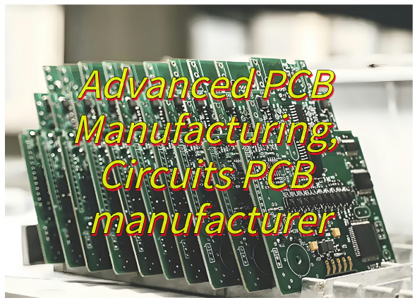
As a premier advanced circuits PCB manufacturer, EBest Circuit (Best Technology) stands out with exceptional technical capabilities and unmatched delivery speed. Our cutting-edge production facilities specialize in high-density interconnect (HDI), rigid-flex, and high-frequency PCBs, achieving precision up to 3/3mil line/space with 12+ layer configurations. What truly differentiates us is our commitment to rapid turnaround – offering 15-day standard production cycles (30% faster than industry norms) and expedited 48-hour prototype services without compromising IPC Class 3 quality standards. With 10,000+ sqm of manufacturing space and automated optical inspection systems, we maintain 99.97% on-time delivery rates for global clients across aerospace, medical, and automotive sectors. Our RoHS/REACH compliant materials, coupled with dedicated export account managers and free DFM analysis, ensure seamless cross-border collaboration. Having successfully executed 5,000+ complex projects with <0.5% defect rates, we combine US compliance certifications with China-based cost efficiency – delivering technically superior boards that accelerate your product development timelines while meeting stringent international reliability requirements. Welcome to contact us: sales@bestpcbs.com.
What Is Advanced PCB Manufacturing?
Advanced PCB manufacturing refers to a sophisticated approach in the production of printed circuit boards. It encompasses the use of cutting – edge techniques, high – end materials, and state – of – the – art equipment to create PCBs that meet the demanding requirements of modern electronics. Unlike traditional manufacturing methods, advanced PCB manufacturing is tailored to produce boards with higher precision, better performance, and enhanced reliability. These PCBs are often used in complex applications such as aerospace, medical devices, high – performance computing, and telecommunications, where standard PCBs may not suffice.
What Materials Are Used in Advanced PCB Manufacturing?
- High-Performance Laminate Materials: Materials like Rogers RT/duroid series are commonly used in advanced PCB manufacturing. They offer excellent electrical properties, including low dielectric loss and stable dielectric constant, which are crucial for high – frequency applications.
- Copper Foil: High – purity electrolytic copper foil is preferred. It provides good electrical conductivity and can be processed to achieve fine line widths and spaces required in advanced designs.
- Prepregs: Prepregs, which are partially cured epoxy – impregnated fiberglass sheets, are used to bond the layers of a multi – layer PCB. Advanced prepregs have improved flow and adhesion properties for better layer – to – layer bonding.
- Thermally Conductive Materials: In applications where heat dissipation is critical, thermally conductive materials are incorporated. These materials help transfer heat away from components, preventing overheating and improving the overall lifespan of the PCB.
- Halogen-Free Materials: With the increasing focus on environmental sustainability, halogen – free materials are becoming more popular in advanced PCB manufacturing. They offer similar performance to traditional materials but are more environmentally friendly.
- Specialty Dielectric Materials: For specific applications, such as microwave and millimeter – wave circuits, specialty dielectric materials with unique properties are utilized. These materials can be customized to meet the exact electrical requirements of the design.
What Are the Technologies in Advanced PCB Manufacturing?
- High-Density Interconnect (HDI) Technology: Using laser-drilled microvias and fine-pitch routing, HDI technology can increase PCB component density by more than 30%, with line width/pitch reaching 50μm, suitable for highly integrated devices such as mobile phones and servers.
- Multilayer PCB Technology: Multilayer boards can achieve up to 40 layers of stacking, optimize power supply through inner power/ground layers, and reduce interference through differential signal layers. They are often used in complex signal scenarios such as aerospace and high-end servers.
- Flexible and Rigid-Flex PCB Technology: The minimum bending radius of flexible boards can reach 0.5mm, and rigid-flexible boards support more than 200,000 bends. They are widely used in dynamic assembly environments such as folding screen mobile phones and surgical robots.
- 3D Printing for PCBs: 3D printing can achieve vertical interconnection and embedded device integration, and the proofing cycle is shortened from 7 days to 24 hours, which is suitable for small-batch customization and concept verification stages.
- Electroplating and Surface Finishing Technologies: ENIG process provides nickel layer of more than 50μm + gold layer of 0.05μm, and OSP film thickness of 0.2-0.5μm, both of which can ensure welding yield> 99.5%, and improve PCB service life.
- Automated Optical Inspection (AOI) and X-Ray Inspection: AOI inspection accuracy reaches 50μm, and X-rays penetrate 5mm thick boards to detect internal solder joints. The combination of double inspections can increase the defect detection rate to 99.9%, ensuring the quality of shipment.
How Does Advanced PCB Manufacturing Improve Signal Integrity?
Precise Trace Routing
- In actual production, laser direct imaging (LDI) technology can be used to achieve high-precision line etching, and the line width tolerance can be controlled within ±5μm. During design, the automatic routing and manual adjustment functions of the electronic design automation (EDA) software are used, combined with equal length rule constraints, to ensure that the length of the key signal path is consistent. For example, in the design of high-speed DDR memory circuits, the routing length deviation of the data line and the clock line is precisely controlled within 5mil, effectively reducing signal reflection and crosstalk.
Layer Stack-up Optimization
- Select appropriate dielectric materials according to product functions, such as Rogers RT/duroid series materials in high-frequency communication PCBs, whose low dielectric constant and low loss characteristics can reduce signal attenuation. When designing the stacked structure, a symmetrical stacking scheme is used to tightly couple the power layer and the ground layer, with the signal layer in the middle. For example, for a 10-layer PCB, it can be designed as a signal-ground-signal-power-ground-signal-power-ground-signal-ground-signal-ground structure, which can effectively suppress electromagnetic interference (EMI).
High-Quality Dielectric Materials
- In the manufacturing of 5G base station PCBs, low-loss dielectric materials such as Nelco N4000-13SI are often used, and its loss tangent value in the 28GHz frequency band is only 0.0035. During the production process, the thickness uniformity of the dielectric layer is strictly controlled, and the thickness tolerance of the dielectric layer is ensured to be within ±3% through the optimization of the pressing process parameters to ensure the integrity of the signal during transmission.
Proper Grounding and Shielding
- A multi-point grounding design is adopted, and ground vias are set at a certain distance on the PCB board, and the ground vias are connected to the main ground plane to form a low-impedance grounding path. For sensitive signal areas, a metal shielding cover is used for physical shielding, and the shielding cover is well connected to the ground plane of the PCB through welding pins. For example, in RF front-end circuits, individual shielding of modules such as power amplifiers and mixers can reduce external interference by more than 20dB.
Microvia Technology
- In high-density interconnect (HDI) PCB manufacturing, laser drilling technology is used to make microvias, and the aperture is usually between 50-100μm. After drilling, chemical copper plating is performed to ensure that the thickness of the copper layer on the hole wall is uniform and controlled at 18-25μm. This microvia structure can reduce signal delay by more than 15% in high-speed digital circuits compared to traditional through holes, and is particularly suitable for PCB design of miniaturized electronic products such as smartphones.
Controlled Impedance Design
- When producing controlled impedance PCBs, the impedance value is precisely controlled by adjusting the line width, dielectric thickness, and copper foil thickness. For example, for a microstrip line with a 50Ω impedance, when the dielectric thickness is 0.254mm and the copper foil thickness is 18μm, the line width needs to be controlled at around 0.28mm. During the production process, a time domain reflectometer (TDR) is used to detect impedance in real time and correct lines that exceed the tolerance range (±10%) to ensure the reliability of signal transmission.
How to Select An Advanced Circuit PCB Manufacturer?
Below are methods about how to select an advanced circuit PCB manufacturer:
- Experience and Reputation: Give priority to manufacturers with more than 3 years of mass production experience in advanced PCB manufacturing fields such as HDI, blind and buried vias, and rigid-flex boards. Check their customer reviews, list of partner companies, and industry reputation, and focus on the number of long-term partners.
- Technical Expertise: Confirm that the manufacturer has mastered core processes such as laser drilling (minimum aperture ≤ 0.1mm), high-order blind and buried vias, and mixed-pressed multilayer boards (≥ 20 layers). Require a list of process capabilities, including parameters such as minimum line width/line spacing and impedance control accuracy.
- Quality Assurance System: Verify whether the AQL 1.0 sampling standard is implemented, and AOI automatic optical inspection and X-Ray inner layer inspection equipment are equipped. Request SPC (statistical process control) reports and process capability index (CPK≥1.33) data for the past 3 months.
- Production Capacity: Assess whether the monthly production capacity meets demand and confirm that there is a double-shift or three-shift production mode. Requires a standardized delivery commitment, such as 7-10 working days for regular orders and 3-5 working days for expedited orders.
- Cost – Effectiveness: Compare quotations from at least 3 manufacturers, focusing on the full-cycle cost including engineering fees, testing fees, and NRE (one-time engineering costs). Focus on evaluating the unit price reduction during mass production, and require a step-by-step quotation plan.
- Customer Support: Confirm whether a full-time project engineer is equipped to provide 24-hour technical response service. Requires a complete DFM (Design for Manufacturability) analysis report, covering design optimization suggestions and potential risk warnings.
- Certifications: Verify whether it has ISO 9001:2015, IPC – 6012 Class 3 certification, and RoHS 2.0, REACH environmental compliance certification. Requires a scanned copy of the original certificate and the latest audit report.
- Innovation and Research & Development: Investigate whether there is an R&D laboratory, and the annual R&D investment accounts for no less than 5%. Understand its breakthrough cases in cutting-edge technologies such as high-speed material applications (such as Rogers, Isola), high-frequency circuit processing, etc.
- Supply Chain Management: Confirm the stable supplier list of key materials (copper foil, PP sheet, solder mask ink) and establish at least 2 alternative suppliers. It is required to provide a material batch traceability system to ensure that the entire production process can be checked.
- Portfolio of Past Projects: Detailed review of cases similar to your own products, including parameters such as product type, number of layers, and process difficulty. It is required to provide customer acceptance reports and performance test data for more than 3 projects of the same type.
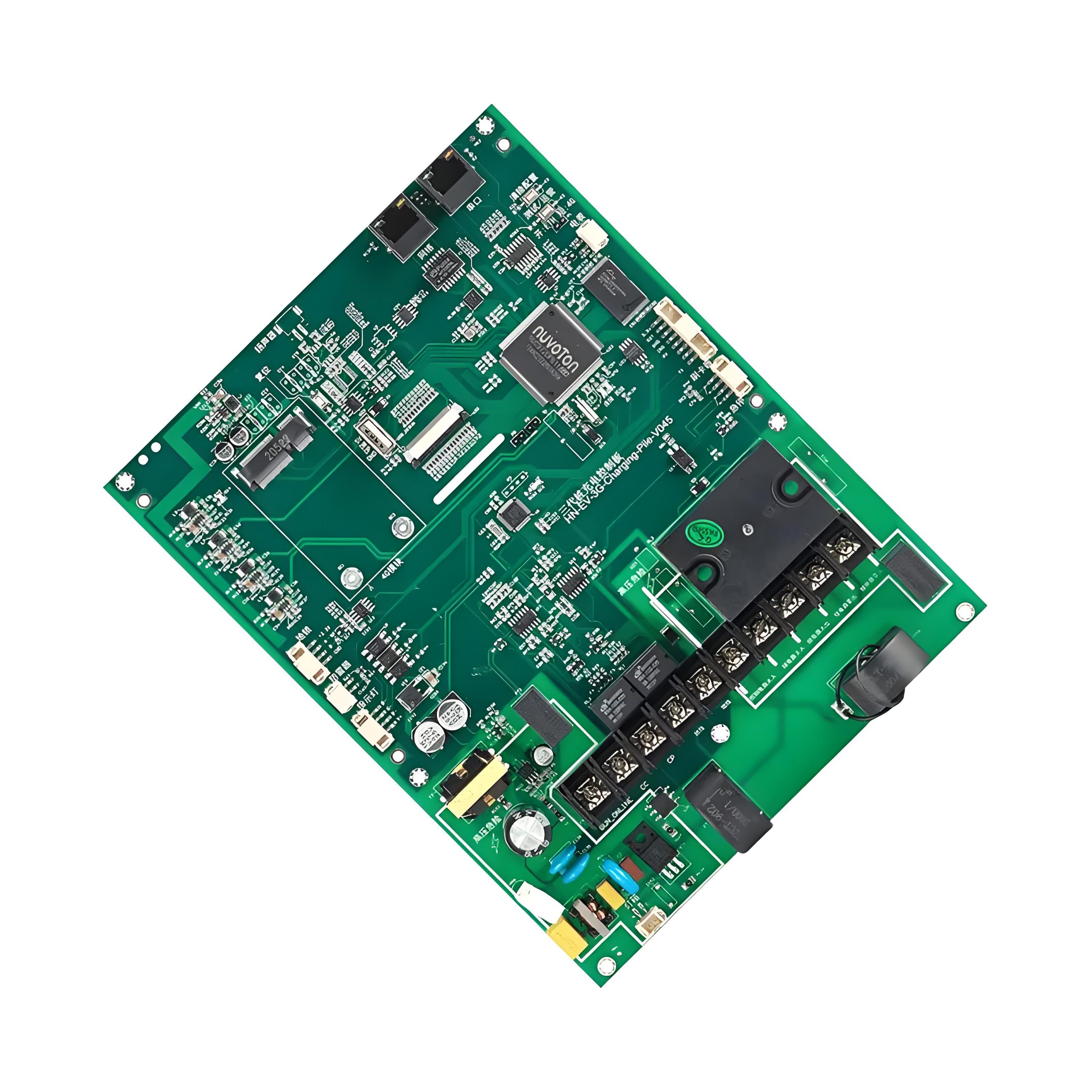
What Production Capabilities Should Advanced PCB Manufacturers Have?
High-Precision Manufacturing Equipment: Advanced PCB manufacturers must utilize cutting-edge production equipment to process boards with fine line widths, small aperture diameters, and high-density interconnects. For example, laser drilling machines can create microvias as small as one-third the diameter of a human hair; high-precision milling machines achieve ±5 micrometer line accuracy; and advanced electroplating equipment ensures uniform copper layers in plated-through holes, eliminating fracture risks.
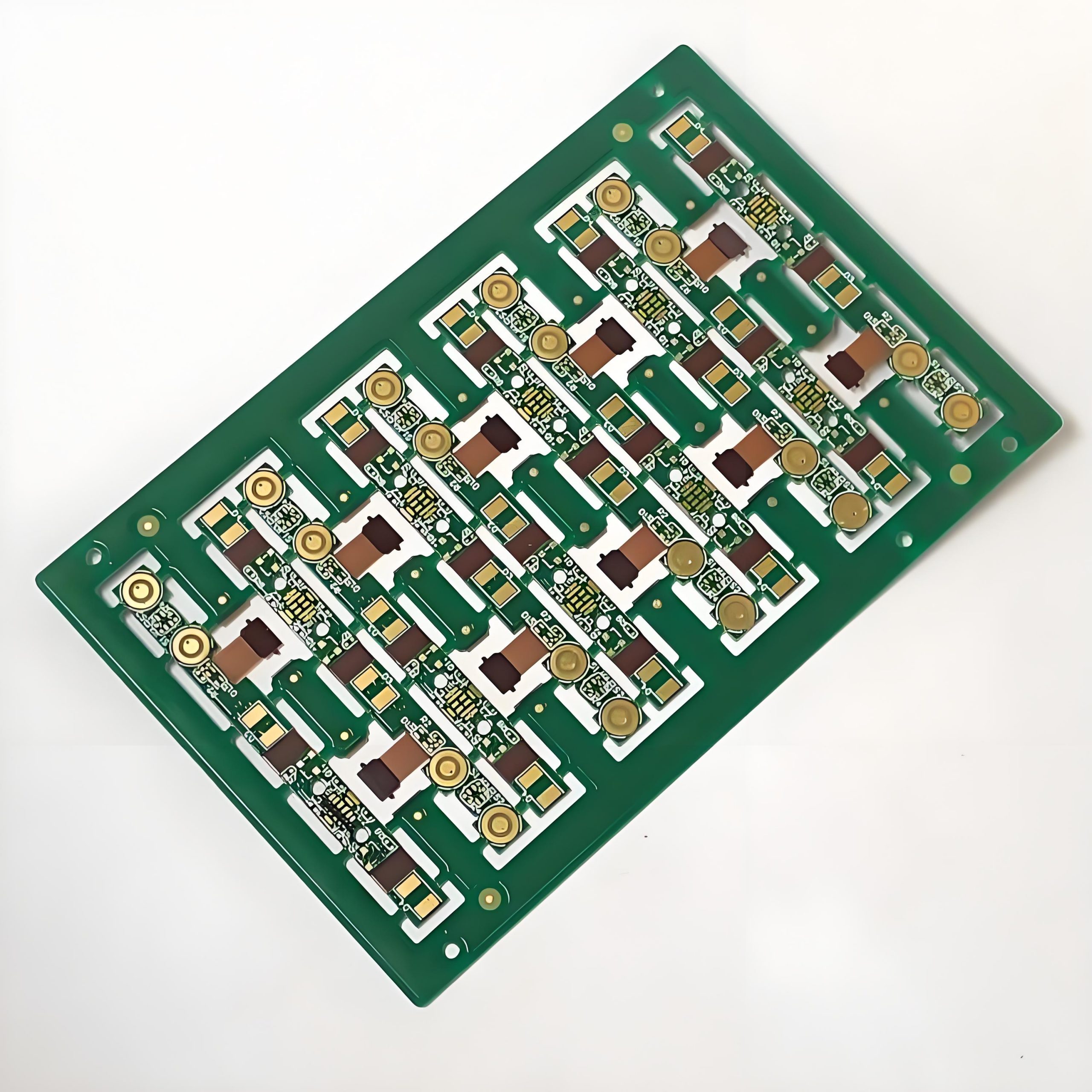
Multilayer PCB Production: Producing over 20-layer multilayer PCBs hinges on precise lamination and bonding processes. Vacuum hot pressing technology aligns each layer with micrometer-level accuracy, while epoxy prepreg ensures seamless bonding to guarantee zero-delay, zero-loss signal transmission between layers.
Rigid-Flex PCB Manufacturing: Flexible (FPC) and rigid-flex PCB production requires mastery of polyimide and other flexible substrate properties. CNC bending machines achieve millimeter-precision folding, while pulse hot pressing ensures robust bonding between rigid and flexible sections, enabling applications in wearable devices and other complex designs.
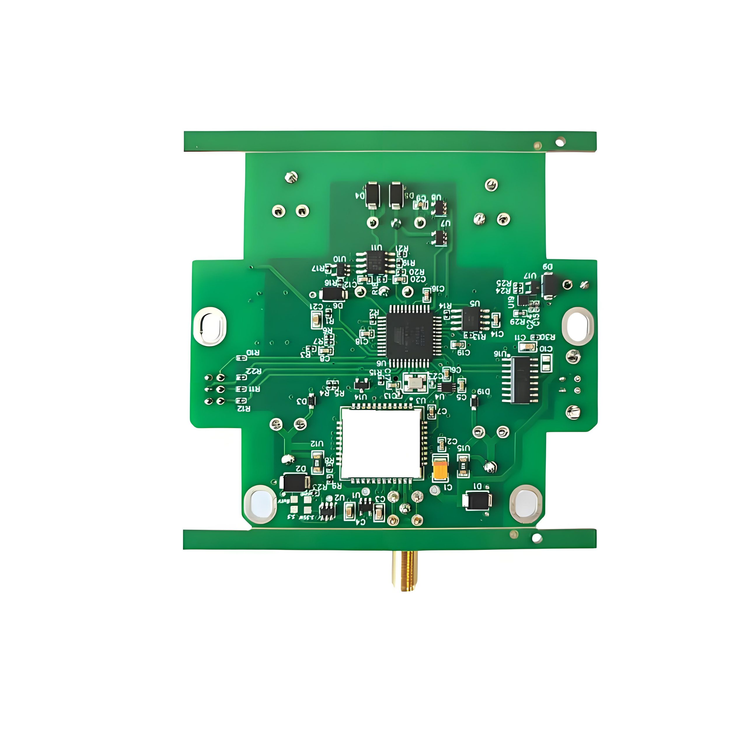
Advanced Surface Mount Technology (SMT): SMT assembly demands capability to place 0201 components (0.6×0.3mm) and handle 1000+ pin BGA packages. Fully automated pick-and-place machines achieve over 100,000 components per hour, with X-ray inspection ensuring solder joint quality.
Rapid Prototyping Services: For time-sensitive product development, top-tier manufacturers can deliver single/double-sided PCB prototypes within 48 hours, with multilayer board prototyping compressed to 7 days. Digital lithography (LDI) exposure and chemical etching rapidly convert designs into physical boards.
Automated Production Workflow: From automated material handling and intelligent placement to AOI optical inspection, full automation reduces human error by over 80%. For example, automated optical inspectors scan 3,000 solder joints per minute, precisely detecting defects like cold joints or shorts.
Thermal Management Solutions: High-power PCBs integrate heat sinks, copper pillars, and embedded copper blocks, with thermal vias reducing localized hotspot temperatures by over 30°C, ensuring long-term stability.
Comprehensive Testing Systems: Flying probe testers detect opens/shorts, while functional test benches simulate real-world scenarios. Combined with salt spray, thermal cycling, and 20+ reliability tests, every PCB undergoes rigorous validation.
Customization Capabilities: Flexible design of blind/buried vias, impedance matching optimization, and DFM (Design for Manufacturability) analysis raise yields by over 20% through collaborative design with clients.
Environmentally Compliant Production: Strict adherence to RoHS directives eliminates lead, mercury, and other hazardous substances. Water-based inks and cyanide-free electroplating reduce wastewater to potable standards, achieving green manufacturing.
How Do Top Advanced Circuits PCB Manufacturers Ensure Quality Control?
- Incoming Material Inspection: All incoming materials, including copper foil, laminates, and components, are thoroughly inspected to ensure they meet the required quality standards. This includes checking for physical defects, electrical properties, and compliance with specifications.
- Process Control: During the manufacturing process, strict process control measures are implemented. This includes monitoring and controlling parameters such as temperature, pressure, and chemical concentrations to ensure consistent quality.
- In – Process Inspection: Regular in – process inspections are carried out at various stages of production. This includes inspecting the drilled holes, etched traces, and plated surfaces to detect any defects early and prevent them from propagating to the next stage.
- Automated Optical Inspection (AOI): AOI systems are used to automatically inspect the PCB surface for defects such as missing components, misaligned components, and soldering defects. These systems can quickly and accurately detect a wide range of surface – level defects.
- X – Ray Inspection: X – ray inspection is used to detect internal defects, such as voids in solder joints, open circuits, and shorts in multilayer PCBs. This non – destructive testing method provides detailed information about the internal structure of the PCB.
- Electrical Testing: Electrical testing is performed to ensure that the PCBs meet the required electrical specifications. This includes testing for continuity, insulation resistance, and impedance.
- Functional Testing: Functional testing is carried out to verify the functionality of the PCBs in a real – world or simulated environment. This includes testing the performance of the circuits, the interaction between components, and the overall system functionality.
- Reliability Testing: Reliability testing, such as temperature cycling, humidity testing, and vibration testing, is conducted to assess the long – term reliability of the PCBs. This helps to identify potential failure modes and improve the design and manufacturing processes.
- Quality Management System (QMS): Top advanced PCB manufacturers have a well – established QMS in place. This includes quality planning, quality control, quality assurance, and quality improvement processes to ensure continuous improvement in product quality.
- Employee Training and Certification: Employees are trained and certified in various aspects of advanced PCB manufacturing and quality control. This ensures that they have the necessary skills and knowledge to perform their tasks accurately and maintain high – quality standards.
What Is the Difference Between Advanced PCB and Universal PCB Manufacturing?
- Complexity of Design: Advanced PCBs often have more complex designs with higher component density, smaller feature sizes, and multiple layers. Universal PCBs, on the other hand, typically have simpler designs and are suitable for less demanding applications.
- Materials Used: Advanced PCB manufacturing uses high – performance materials with superior electrical, thermal, and mechanical properties. Universal PCB manufacturing may use more common and cost – effective materials that meet basic requirements.
- Manufacturing Technologies: Advanced PCB manufacturing employs advanced technologies such as HDI, 3D printing, and flexible PCB technology. Universal PCB manufacturing usually relies on traditional manufacturing methods, which may not be able to achieve the same level of precision and complexity.
- Signal Integrity: Advanced PCBs are designed with a greater focus on signal integrity, using techniques such as controlled impedance design and advanced grounding and shielding. Universal PCBs may not require the same level of signal integrity optimization.
- Production Volume: Advanced PCBs are often produced in smaller volumes, especially for prototype and high – end applications. Universal PCBs are more commonly produced in large volumes for mass – market products.
- Cost: Due to the use of advanced materials, technologies, and the higher level of precision required, advanced PCBs are generally more expensive to manufacture. Universal PCBs are more cost – effective, making them suitable for applications where cost is a major consideration.
- Quality Control Requirements: Advanced PCB manufacturing has more stringent quality control requirements to ensure the reliability and performance of the PCBs. Universal PCB manufacturing may have less rigorous quality control processes, depending on the application.
- Application Areas: Advanced PCBs are used in high – end applications such as aerospace, medical, and telecommunications, where performance, reliability, and miniaturization are critical. Universal PCBs are commonly used in consumer electronics, household appliances, and other general – purpose applications.
- Design Flexibility: Advanced PCB manufacturing offers greater design flexibility, allowing for the creation of customized PCBs to meet specific requirements. Universal PCB manufacturing may have more limited design options due to the use of standard manufacturing processes.
- Lead Time: The production lead time for advanced PCBs is usually longer due to the complexity of the manufacturing process and the need for more detailed quality control. Universal PCBs can often be produced more quickly, especially in large volumes.
Conclusion
In conclusion, advanced PCB manufacturing is a vital and evolving field in modern electronics, offering benefits like enhanced signal integrity and the capacity for complex, customized PCBs for high – end uses. Grasping the materials, technologies, and production aspects is crucial for creating high – performance electronics. When choosing an advanced circuit PCB manufacturer, factors such as experience, technical know – how, quality control, and production capabilities matter. Recognizing the differences between advanced and universal PCB manufacturing aids in making project – specific decisions. For high quality advanced PCB manufacturing services, contact sales@bestpcbs.com for a quote; our team is committed to using its experience and expertise to fulfill all your needs.