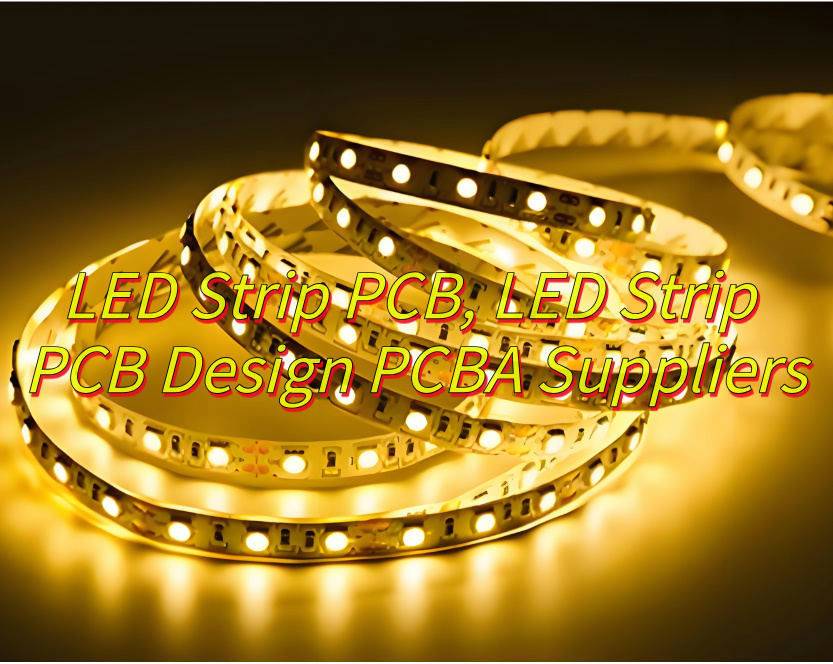
Want to know how LED Strip PCB powers innovation? Dive into its materials, applications, design tips, assembly steps, supplier selection, precision control, and ultra-thin customization.
EBest Circuit (Best Technology) is a leading LED Strip PCB design PCBA manufacturer, offering end-to-end solutions with superior engineering capabilities. Our state-of-the-art automated SMT production lines ensure high-precision manufacturing at scale, while our 24-hour rapid prototyping service enables lightning-fast turnaround for design validation. Specializing in high-performance LED PCB designs, we integrate advanced thermal management solutions (40% more efficient than standard boards), precise optical alignment (0.1mm tolerance), and flexible hybrid layouts to optimize light uniformity and durability. Every product undergoes rigorous 5-stage quality inspections including AOI, X-ray, and functional testing, achieving 99.9% defect-free reliability. With UL/CE/RoHS certified materials and 10,000+ cycle bend-tested flexible PCBs, we guarantee long-term performance. Our one-stop service covers design optimization, DFM analysis, and fast-track production—delivering prototypes within 24 hours and mass production in 7-12 days. Trust our decade of expertise to transform your LED lighting concepts into market-ready products with unmatched speed-to-market and cost efficiency. Welcome to contact us if you have any request for LED strip PCB: sales@bestpcbs.com.
What Is LED Strip PCB?
A LED strip PCB is a specialized printed circuit board designed to mount and power light-emitting diodes (LEDs) in a linear array. These boards feature conductive copper traces that deliver electricity to individual LED chips, often incorporating resistors for current regulation and sometimes integrated circuits for advanced control like dimming or color changing. Flexible LED strip PCBs use bendable materials like polyimide, allowing them to conform to curved surfaces, while rigid versions employ sturdy substrates such as FR4 for stability. The design ensures proper thermal dissipation through materials like aluminum or copper layers to prevent overheating. LED strip PCBs enable uniform light distribution by precisely spacing LEDs along the board, with options for single-color, RGB, or addressable configurations. They are widely used in decorative lighting, architectural accents, task illumination, and automotive lighting due to their efficiency and versatility. Manufacturers assemble components using surface-mount technology (SMT) and apply protective coatings for waterproofing or insulation when needed. LED strip PCBs provide a reliable foundation for various lighting applications, balancing performance, durability, and ease of installation.

What Is Material of LED Strip PCB?
Materials of LED Strip PCB:
- Flexible Substrate: Polyimide (PI) or polyester (PET) films form the bendable base for flexible LED strip PCBs, enabling installation on curved surfaces without cracking circuitry.
- Rigid Substrate: FR4 fiberglass-reinforced epoxy laminates provide structural rigidity for stationary LED strip PCBs, ensuring durability in fixed lighting setups.
- Conductive Layer: Copper foil (1-oz to 4-oz thickness) creates electrical pathways on LED strip PCBs, optimized for current distribution and minimized voltage drop across the strip.
- Thermal Management: Aluminum-core or metal-core PCB (MCPCB) materials dissipate heat in high-power LED strip PCBs, extending LED lifespan by preventing thermal overload.
- Surface Finish: Immersion silver, OSP (Organic Solderability Preservative), or ENIG (Electroless Nickel Immersion Gold) coatings protect copper traces on LED strip PCBs from oxidation and enhance solderability.
- Protective Coating: Silicone or epoxy resin encapsulates LED strip PCBs, providing water resistance (IP65-IP68) and mechanical protection while maintaining optical clarity.
- Adhesive Layer: Acrylic-based pressure-sensitive adhesives enable peel-and-stick installation of LED strip PCBs onto diverse surfaces like walls, vehicles, or furniture.
- Solder Mask: LPI solder mask insulates copper traces on LED strip PCBs, preventing short circuits and defining component placement zones.
- Component Materials: Surface-mount LEDs (SMD chips) and resistors are bonded to LED strip PCBs using lead-free SAC305 solder, complying with global environmental standards.
- Stiffener: Fiberglass or nylon stiffeners reinforce cut points and connector areas on LED strip PCBs, preventing flex damage during installation or maintenance.
- Material choices in LED strip PCBs prioritize electrical efficiency, thermal performance, environmental adaptability, and cost-effectiveness for diverse lighting applications.

What Are Application of LED Strip PCB?
Application of LED strip PCB:
- Architectural Lighting: LED strip PCBs illuminate ceilings, coves, and under-cabinet spaces in modern buildings, offering energy-efficient and customizable lighting solutions for contemporary interiors.
- Retail Displays: LED strip PCBs enhance product visibility in stores through dynamic display lighting, enabling adjustable brightness and color-changing effects to attract customers.
- Automotive Interiors: LED strip PCBs are integrated into vehicle dashboards, door panels, and ambient footwell lighting, combining aesthetics with safety standards in automotive design.
- Entertainment Lighting: LED strip PCBs create immersive lighting effects in stage designs, concerts, and film sets, synchronized with music or visual content for dynamic performances.
- Industrial Lighting: LED strip PCBs provide durable, low-maintenance lighting in machinery, control panels, and emergency exit pathways, ensuring reliability in harsh operational environments.
- Residential Decor: LED strip PCBs offer sleek, hidden lighting solutions in kitchens, living rooms, and bedrooms, enabling subtle ambiance through installations behind furniture or along staircases.
- Medical Lighting: LED strip PCBs ensure uniform light output in operating rooms and examination lamps, meeting sterile equipment design requirements while supporting healthcare environments.
- Smart Homes: LED strip PCBs with IoT connectivity allow remote control via mobile apps or voice assistants, enabling smart scheduling, color adjustments, and power management.
- Aquarium Lighting: LED strip PCBs simulate natural daylight cycles in aquariums and terrariums, adjustable spectrum and intensity controls support plant growth and animal habitats.
- Public Infrastructure: LED strip PCBs guide passengers in airports and subways through wayfinding systems and artistic installations, blending functionality with visual appeal in public spaces.

How to Optimize the Design Layout of LED Strip PCB?
Here are methods about how to optimize the design layout of LED strip PCB:
- Simplify Circuit Routing: Reduce unnecessary traces and layers by consolidating power and ground paths. Use single-layer or double-layer PCBs instead of multi-layer designs for cost-effective LED strip PCB manufacturing.
- Optimize Component Placement: Arrange LEDs and resistors in linear patterns to minimize copper usage and simplify soldering processes. Avoid overcrowding components to prevent assembly errors and rework costs.
- Standardize PCB Dimensions: Adopt industry-standard widths and lengths for LED strip PCBs to streamline production tooling and reduce material scrap rates during cutting and panelization.
- Use Cost-Effective Substrates: Select FR-4 or CEM-1 materials for rigid LED strip PCBs instead of high-cost alternatives like aluminum or ceramic. For flexible designs, choose thin polyimide films with adhesiveless bonding to lower material expenses.
- Reduce Copper Thickness: Specify 1oz (35μm) copper foil instead of thicker options for non-high-current applications. This reduces etching time and material costs while maintaining sufficient conductivity for LED strips.
- Implement Surface Mount Technology (SMT): Utilize SMT LEDs and passive components to eliminate through-hole drilling and manual assembly steps, enabling automated pick-and-place production for faster throughput and lower labor costs.
- Merge Voltage Rails: Combine low-voltage and high-voltage sections on the same LED strip PCB where possible to reduce connector counts and simplify power supply designs, cutting component procurement expenses.
- Minimize Via Usage: Limit plated-through holes (PTHs) by rerouting traces or using jumpers. This reduces drilling and plating costs while improving manufacturing yield for LED strip PCBs.
- Adopt Panelized Production: Design LED strip PCBs in array formats compatible with standard panel sizes (e.g., 500mm x 500mm) to maximize SMT line efficiency and reduce per-unit setup costs.
- Leverage Design for Manufacturability (DFM) Tools: Use DFM software to identify and resolve design issues early, such as trace spacing violations or solder mask misalignment, preventing costly redesigns and production delays.
- Simplify Thermal Management: Replace bulky heat sinks with copper pads or thermal vias directly beneath LEDs to dissipate heat efficiently, reducing material and assembly costs for LED strip PCBs.
- Eliminate Redundant Features: Remove non-functional elements like unused test points or decorative logos from the PCB layout to save etching and inspection time during manufacturing.
- Centralize Power Distribution: Use bus bars or thick copper traces for power lines instead of multiple thin wires, reducing component count and assembly complexity while improving reliability.
- Optimize Solder Mask Openings: Align solder mask dams with SMD pad sizes to prevent solder bridging without over-masking, minimizing rework and material waste in LED strip PCB production.
- Collaborate with Contract Manufacturers: Share design files with PCB fabricators early to refine layouts for their equipment capabilities, avoiding costly adjustments during prototyping or mass production.

What Is Assembly Process of LED Strip Flexible PCB?
Here are assembly process of LED strip flexible PCB:
1. Design and Material Preparation:
- Engineers use PCB design software (e.g., Altium Designer, KiCad) to finalize the layout of LEDs, power traces, and circuitry on flexible substrates like polyimide (PI) or polyester (PET). Designs prioritize signal integrity, thermal management, and flexibility for applications such as automotive dashboards or architectural cove lighting.
- Materials are prepared, including rolled copper-clad laminates (CCLs) with adhesiveless bonding layers, surface-mount device (SMD) LED chips (e.g., 2835, 5050 models), and driver integrated circuits (ICs). Substrates undergo laser cutting or CNC routing to achieve precise dimensions.
2. Pre-Treatment of Flexible PCBs (FPC):
- FPC boards are baked at 80–100°C for 4–8 hours to remove moisture absorbed during storage, preventing defects like popcorning during soldering.
- Specialized carriers (e.g., synthetic stone or aluminum plates) and定位 templates secure FPCs during surface mount technology (SMT) processes, ensuring alignment accuracy within ±0.05mm.
3. Solder Paste Printing:
- A stainless-steel stencil with laser-cut apertures aligns with the FPC’s solder pads. Solder paste (e.g., SAC305 alloy) is printed using a semi-automatic or fully automatic stencil printer, achieving consistent deposition for 0.3mm pitch components.
4. Surface Mount Technology (SMT) Placement:
- High-speed pick-and-place machines (e.g., Yamaha YSM20R, Siemens SIPLACE) mount SMD LED chips, resistors, and capacitors using vision systems with ±0.1mm precision. For example, a single line may install 300 LEDs per minute on 500mm-long strips for high-resolution displays.
- Nitrogen-assisted reflow ovens melt solder paste at controlled temperatures (245–265°C for lead-free alloys), forming reliable joints while minimizing thermal stress on PI substrates.
5. Through-Hole Component Insertion (If Required):
- For components like connectors or terminals, automated insertion machines place parts into plated-through holes (PTHs). Selective soldering systems apply wave soldering to PTHs while masking SMT components to prevent damage.
6. Manual Assembly and Rework:
- Technicians use microscopes and precision soldering irons to correct minor defects like tombstoned LEDs or solder bridges. Hot air rework stations reflow components without overheating adjacent areas.
7. Conformal Coating and Encapsulation:
- A thin layer of silicone or polyurethane conformal coating is applied via selective spraying to protect against moisture, dust, and vibration. For outdoor or harsh-environment LED strips, potting compounds (e.g., epoxy resins) encapsulate components for IP67/IP68 ratings.
8. Electrical and Functional Testing:
- Post-assembly boards undergo automated optical inspection (AOI) to detect solder voids or missing components.
- Functional tests validate brightness (e.g., 5000 nits), color accuracy (95% NTSC), and uniformity across 2mm pixel pitches using integrating spheres and spectroradiometers.
9. Final Assembly and Packaging:
- Flexible strips are connected to rigid headers or connectors using cold welding or conductive adhesives, ensuring mechanical stability during bending.
- Products are rolled onto anti-static spools or packaged in ESD-safe boxes with silica gel to prevent moisture damage during transport.
10. Quality Assurance and Aging Tests:
- Aging tests run strips for 8–24 hours under voltage to identify early failures.
- Environmental tests (e.g., thermal cycling from -40°C to 85°C, 95% RH humidity) simulate real-world conditions to ensure long-term reliability.
How to Select LED Strip PCB Design PCBA Suppliers?
Here are steps about how to select LED strip PCB design PCBA suppliers:
Evaluate Technical Expertise:
- Prioritize suppliers with experience in LED strip flexible PCB and LED surface mount light PCB manufacturing. Look for certifications like ISO 9001, ISO 14001, and IPC-A-610 compliance to ensure adherence to industry standards for soldering and assembly.
Assess Production Capacity:
- Verify the supplier’s ability to handle your volume requirements. Check if they offer automated SMT lines for high-speed LED placement (e.g., 30,000 components/hour) and flexible PCB lamination capabilities for ultra-thin (≤0.2mm) substrates.
Review Material Sourcing:
- Ensure the supplier uses premium materials like polyimide (PI) films, SAC305 solder paste, and high-brightness SMD LEDs (e.g., 2835, 5050 models). Request material certificates and conflict-free mineral sourcing policies.
Inspect Quality Control Measures:
- Require details on their testing protocols, including AOI (Automated Optical Inspection), X-ray for BGA/QFN components, and burn-in tests. Ask for sample inspection reports and failure rate data (e.g., ≤0.1% defect rate).
Request Prototyping and NPI Support:
- Choose suppliers offering DFM (Design for Manufacturability) reviews and rapid prototyping (e.g., 3–5 days turnaround). Evaluate their ability to iterate designs based on thermal simulations and light uniformity tests.
Check Compliance and Certifications:
- Confirm compliance with safety standards like UL, CE, and RoHS for LED lighting products. For automotive applications, ensure IATF 16949 certification and AEC-Q102 qualification for LED components.
Analyze Cost Structure:
- Compare quotes for NRE (Non-Recurring Engineering) fees, tooling costs, and per-unit pricing. Beware of hidden charges for engineering changes or expedited shipping. Aim for a balance between cost and value-added services.
Assess Supply Chain Resilience:
- Inquire about their inventory management for critical components (e.g., LED drivers, capacitors) and contingency plans for material shortages. Diversified sourcing from multiple regions reduces lead time risks.
Review Customer References:
- Contact references from similar industries (e.g., automotive lighting, consumer electronics) to gauge on-time delivery performance, responsiveness to issues, and post-sales support.
Negotiate Contract Terms:
- Finalize agreements covering intellectual property protection, warranty periods (e.g., 2–3 years), liability clauses, and escalation procedures for disputes. Include SLAs (Service Level Agreements) for lead times and defect rates.
How to Control High-Density LED Strip PCB Mounting Accuracy?
This is how to control high-density LED strip PCB mounting accuracy:
Optimize PCB Layout Design:
- Use advanced PCB design software (e.g., Altium Designer, Cadence Allegro) to precisely define component footprints and trace spacing for LED Strip Flexible PCBs. Maintain a minimum of 0.2mm clearance between SMD LED pads and adjacent traces to prevent solder bridging.
- Implement panelized designs with alignment markers and tooling holes to streamline automated assembly and reduce positional errors during SMT placement.
Leverage High-Precision SMT Equipment:
- Deploy pick-and-place machines with sub-micron accuracy (e.g., ±0.025mm placement tolerance) and multi-camera vision systems to handle 0201/01005-sized LED components.
- Utilize nitrogen-atmosphere reflow ovens to minimize oxidation and ensure consistent solder joint formation, critical for maintaining alignment in high-density LED arrays.
Implement Laser-Cut Stencils for Solder Paste Printing:
- Use laser-cut stainless-steel stencils with electropolished apertures to achieve ±5μm solder paste deposition accuracy. This ensures uniform solder volume for miniature LEDs (e.g., 2835/5050 models) on flexible substrates.
Adopt Advanced Process Control Systems:
- Integrate real-time process monitoring (RPM) tools to track solder paste printing height, placement force, and reflow profiles. Adjust parameters dynamically using AI-driven algorithms to compensate for thermal drift or mechanical wear.
Control Environmental Factors:
- Maintain a 22±2°C temperature and 45±5% RH humidity-controlled cleanroom environment to prevent substrate warpage or electrostatic discharge (ESD) during LED Strip Flexible PCB assembly.
Utilize Carrier Systems for Flexible Substrates:
- Secure flexible PCBs to rigid carriers (e.g., synthetic stone, aluminum) using vacuum chucks or mechanical clamps during SMT. This prevents stretching or misalignment of the polyimide substrate during high-speed component placement.
Perform Post-Assembly Alignment Verification:
- Conduct 3D automated optical inspection (AOI) with multi-angle lighting to detect LED positional deviations ≤0.05mm. Use machine vision algorithms to cross-reference actual positions against CAD design data.
Optimize Conveyor and Handling Systems:
- Equip SMT lines with anti-static conveyors featuring edge-grip transport mechanisms to minimize substrate flexure. Avoid manual handling of populated LED strips to prevent component displacement.
Validate Material Compatibility:
- Source LED Strip Flexible PCB substrates with matched coefficients of thermal expansion (CTE) to SMD components. Test material combinations under thermal cycling (-40°C to 125°C) to ensure dimensional stability.
Implement Statistical Process Control (SPC):
- Collect and analyze SPC data for key processes (e.g., solder paste volume, placement accuracy, reflow profiles). Set control limits (e.g., ±0.03mm for LED X/Y placement) and trigger corrective actions for out-of-spec conditions.
Can Your Factory Customize Ultra-Thin LED Flex PCB?
Yes, our factory excels in manufacturing ultra-thin LED flexible PCBs, leveraging advanced materials and precision processes to deliver boards as thin as 0.1mm while ensuring reliability for demanding applications. We utilize high-performance polyimide substrates and laser drilling technology to achieve microvias down to 50μm, enabling high-density LED arrays with minimal spacing. Our rigorous quality control includes 100% electrical testing, cross-sectional analysis, and environmental durability tests like thermal cycling and dynamic flex testing. With certifications including ISO 9001 and IATF 16949, we guarantee compliance with automotive and industrial standards. Whether for wearables, automotive HUDs, or medical devices, our expertise in miniaturization and reliability ensures your ultra-thin LED Flex PCB designs meet the highest performance and durability expectations.


