

Looking for high-performance LED flood light PCB solutions? This guide covers technical specs, thermal management, manufacturing selection, and cost factors to optimize your lighting projects.
EBest Circuit (Best Technology) as LED PCB flood light aluminum plate manufacturer understands your struggles with thermal management and premature LED failures in harsh environments. Many lighting projects suffer from inconsistent heat dissipation where standard aluminum substrates create hot spots exceeding 150°C, causing 30% faster lumen depreciation. Our engineered solutions address these pain points with 200W/m·K thermal conductivity boards featuring laser-etched heat channels that reduce junction temperatures by 25°C compared to conventional designs. The proprietary dielectric layer withstands 1000+ thermal cycles without delamination while plasma-treated surfaces maintain solder void rates below 3% for reliable electrical connections. Automated optical alignment ensures ±0.1mm component placement accuracy, eliminating uneven heat distribution across the PCB. With in-house testing simulating desert heat and coastal humidity, we guarantee stable performance through 50,000 hours with less than 5% light output degradation. The result is 40% longer product lifespan and elimination of field failures that inflate maintenance costs. Request our thermal simulation dataset to compare performance metrics for your specific operating conditions and lumen requirements: sales@bestpcbs.com.
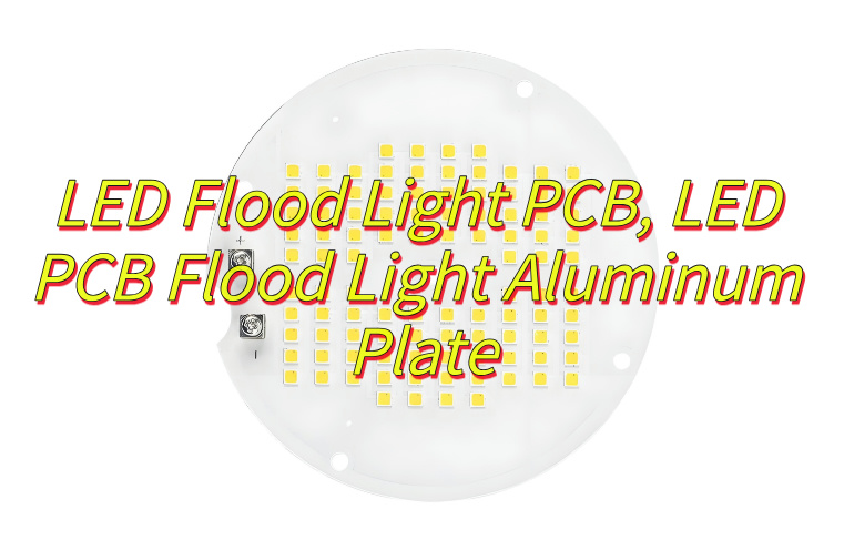
What Is LED Flood Light PCB?
A LED flood light PCB is the specialized circuit board that forms the core component of high-power flood lighting systems. Designed to handle intense thermal and electrical loads, this printed circuit board integrates multiple LED chips while ensuring efficient heat dissipation through its metal core construction, typically aluminum-based for optimal thermal transfer. The board’s architecture combines thick copper traces for current distribution with thermally conductive substrates that pull heat away from sensitive components. Engineers develop these PCBs with durability in mind, incorporating protective finishes that resist environmental factors like moisture and temperature extremes. LED Flood Light PCBs enable uniform light distribution across wide areas through carefully calculated chip placement and circuit design. Their robust construction supports continuous operation in demanding applications such as stadium lighting, industrial complexes, and architectural highlighting. By maintaining stable operating temperatures and electrical performance, these circuit boards directly contribute to extended LED lifespan and consistent luminous output. The integration of thermal vias and heat-spreading layers demonstrates how LED Flood Light PCB technology addresses the unique challenges of high-intensity illumination systems.
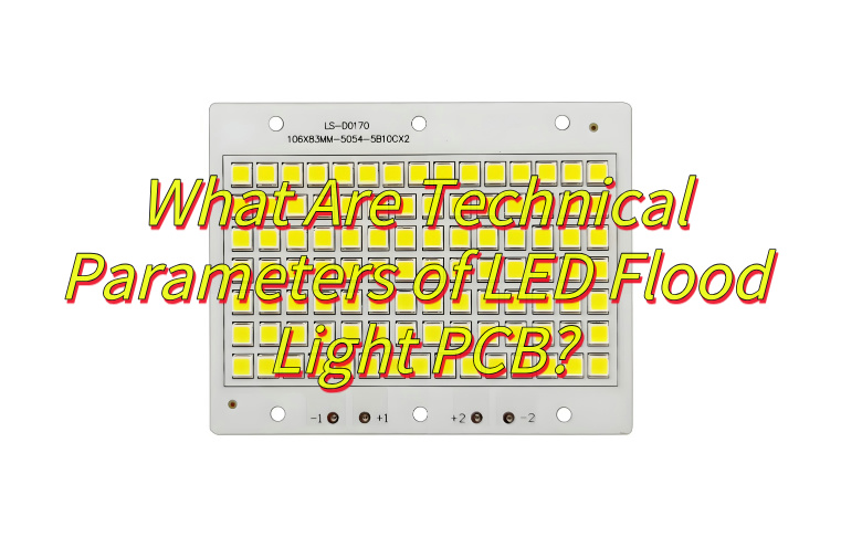
What Are Technical Parameters of LED Flood Light PCB?
Technical Parameters of LED flood light PCB:
- Substrate Material: Aluminum-backed FR4 or metal-core PCB (MCPCB) with 1.6mm thickness for efficient heat dissipation, supporting up to 4W/m·K thermal conductivity.
- Copper Weight: 2oz (70μm) copper layers for high-current applications, ensuring minimal voltage drop across 50W to 500W power ratings.
- Surface Finish: ENIG (Electroless Nickel Immersion Gold) coating with 3–6μm nickel and 0.05–0.15μm gold thickness for solderability and corrosion resistance in outdoor environments.
- Thermal Management: Thermal vias spaced at 1.27mm intervals with 0.3mm diameter, reducing junction-to-board thermal resistance to <1°C/W.
- Dielectric Layer: Prepreg material with 0.1–0.2mm thickness, maintaining 5kV dielectric strength and 288°C glass transition temperature (TG) for lead-free soldering compatibility.
- Solder Mask: LPI solder mask in black or white, with 0.1mm minimum clearance and 8H pencil hardness for UV/weather resistance.
- Component Placement: Supports 0805 to 5050 SMD LED packages and through-hole DIP LEDs, accommodating 0.5mm minimum trace spacing and 0.3mm annular rings.
- Electrical Performance: Impedance control ±10% for 50Ω transmission lines, with 4-layer stack-up isolating power/ground planes to minimize EMI.
- Operating Voltage: Rated for 12V DC to 240V AC input, with surge protection up to 6kV (line-to-ground) and 3kA (8/20μs) transient immunity.
- Environmental Compliance: IP65/IP67 ingress protection, operating temperature range -40°C to +105°C, and 94V-0 flame retardancy per UL 796 standards.
- Mechanical Stability: Bend strength >300MPa and peel strength >1.5N/mm, withstanding 1,000 thermal cycles (-40°C to +125°C) without delamination.
- Optical Performance: Reflective white solder mask (92% reflectivity) and 1.6mm board thickness optimizing light extraction efficiency up to 88%.
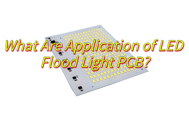
What Are Application of LED Flood Light PCB?
Here are the primary applications of LED flood light PCB in various industries:
- Stadium Lighting Systems: LED Flood Light PCBs provide uniform illumination for sports fields and arenas, with their thermal management capabilities allowing continuous high-intensity operation during night events. The aluminum substrate design prevents overheating during extended matches.
- Industrial Facility Lighting: Manufacturing plants and warehouses utilize these PCBs in high-bay fixtures, where their durable construction withstands vibrations and temperature variations common in industrial environments.
- Architectural Highlighting: Landmark buildings and bridges employ customized LED Flood Light PCBs for aesthetic illumination, with precise thermal vias maintaining color consistency across long façade lighting installations.
- Parking Lot Security Lighting: The weather-resistant properties of LED Flood Light PCBs make them ideal for outdoor parking areas, where they deliver consistent brightness while resisting moisture and temperature extremes.
- Agricultural Growing Operations: Greenhouses use specialized LED Flood Light PCBs with enhanced spectrum control, where the metal-core design supports 18-hour daily operation cycles for plant growth stimulation.
- Airfield Runway Lighting: Aviation applications demand the reliability of LED Flood Light PCBs, with their fail-safe circuitry and robust thermal performance ensuring uninterrupted visibility for aircraft operations.
- Emergency Response Lighting: First responder vehicles and disaster sites deploy these PCBs in portable floodlights, benefiting from their instant-on capability and shock-resistant construction.
- Marine and Dockyard Lighting: Coastal installations utilize corrosion-resistant LED Flood Light PCBs with specialized conformal coatings that protect against saltwater exposure while providing high-lumen output.
- Construction Site Lighting: Temporary work areas implement ruggedized LED Flood Light PCBs that withstand jobsite conditions while delivering energy-efficient illumination for night shifts.
- Entertainment Venue Lighting: Concert stages and outdoor event spaces use high-CRI LED Flood Light PCBs that maintain color accuracy throughout performances, with thermal management preventing brightness fluctuations.
How to Design LED PCB Flood Light Aluminum Plate Avoid Overheating?
Below are how to design LED PCB flood light aluminum plate avoid overheating:
1.Thermal Via Array Optimization
- Deploy 0.3mm diameter vias in a staggered 1.0mm grid pattern beneath LED footprints to maximize heat transfer to the aluminum base.
- Ensure via walls are plated with 25μm copper to minimize thermal resistance (0.15°C/W per via).
- Position vias within 0.5mm of LED thermal pads to create a direct conductive path.
2. Insulated Metal Substrate (IMS) Configuration
- Specify 0.2mm dielectric layers with 1.5W/m·K thermal conductivity for low thermal resistance (<0.25°C/W junction-to-base).
- Validate dielectric integrity using 500V dielectric withstand testing to prevent electrical breakdown.
- Collaborate with PCB manufacturers to ensure ±0.02mm layer registration during lamination.
3. Heat Spreader Geometry Design
- Create 10mm-wide copper flood areas under high-power LEDs (e.g., 50W COB modules) using 2oz copper weight.
- Extend copper planes 15mm beyond LED edges to distribute heat laterally across the aluminum plate.
- Incorporate thermal relief pads (0.5mm spokes) to balance heat dissipation and solderability.
4. Convection Channel Engineering
- Machine 2mm-wide parallel slots between LED clusters using 0.2mm tolerance CNC routing.
- Position channels 5mm from component edges to avoid solder joint stress while maintaining airflow.
- Validate cooling performance via computational fluid dynamics (CFD) simulations at 45°C ambient temperature.
5. Surface Emissivity Enhancement
- Apply brushed anodized finish with 20μm thickness to increase radiative heat dissipation.
- Test surface roughness (Ra 1.6–3.2μm) to optimize emissivity without trapping contaminants.
- Compare infrared (IR) thermal images of anodized vs. bare aluminum prototypes under identical loads.
6. Component Placement Strategy
- Space LEDs at 50mm minimum intervals on 150mm×150mm boards using 3D thermal simulation.
- Group low-power LEDs (≤1W) separately from high-power arrays to prevent thermal coupling.
- Verify placement efficacy with FLIR thermal camera scans after 24-hour continuous operation.
7. Thermal Interface Material (TIM) Application
- Select 0.1mm phase-change pads with 2.5W/m·K conductivity for consistent contact pressure.
- Apply TIM using automated screen printing to achieve 90% coverage uniformity.
- Measure contact resistance with thermocouples placed between PCB and heat sink interfaces.
8. Power Distribution Layout
- Route high-current traces (≥2A) on dedicated inner layers with 1.0mm trace width.
- Isolate power planes from LED footprints using 0.5mm clearance to minimize parasitic heating.
- Confirm current-carrying capacity via IPC-2152 standard calculations for 10°C temperature rise.
9. Environmental Stress Testing
- Conduct 1,000-hour damp heat tests (85°C/85% RH) per IEC 60068-2-78 standards.
- Perform 200 thermal cycles (-40°C to +125°C) with 15-minute dwell times to simulate extreme conditions.
- Monitor solder joint integrity using X-ray inspection after mechanical shock testing (50G, 11ms).
10. Computational Fluid Dynamics (CFD) Validation
- Model natural convection using k-ε turbulence models with 500,000 mesh elements.
- Optimize fin density (8–12 fins per inch) and board tilt angles (15–30°) for airflow efficiency.
- Compare simulation results with wind tunnel data at 2m/s air velocity.
11. Manufacturing Tolerance Control
- Specify ±0.05mm positional accuracy for mounting holes using G-code compensation algorithms.
- Maintain ±3% thickness tolerance on anodized layers via in-process laser scanning.
- Implement statistical process control (SPC) for critical dimensions with CPK ≥1.67 targets.
12. Iterative Design Refinement
- Conduct design of experiments (DOE) varying via density, fin geometry, and TIM type.
- Analyze thermal performance using transient thermal impedance measurements.
- Finalize designs after three prototype iterations with incremental 10–15°C temperature reductions.
How to Choose A LED PCB Flood Light Aluminum Plate Manufacturer?
Below are how to choose a LED PCB flood light aluminum plate manufacturer:
- Check Industry Certifications: Ensure the manufacturer holds ISO 9001 quality management and ISO 14001 environmental certifications. Look for UL 796 or IEC 61249 compliance to guarantee PCB safety in harsh conditions.
- Inspect Production Equipment: Verify the use of advanced CNC machines for precise milling and laser drilling. Automated optical inspection systems ensure defect-free boards with consistent thermal via quality.
- Review Quality Control Processes: Examine thermal cycling and salt spray test results. Cross-section analysis of dielectric layers confirms material uniformity and adhesion strength.
- Evaluate Material Traceability: Request certificates for aluminum alloys and dielectric materials. Traceable supply chains ensure consistent performance across batches.
- Test Customization Capabilities: Submit design files for DFM feedback. Prototype comparisons reveal differences in fin density, anodized finish, and thermal performance.
- Analyze Customer References: Contact previous clients to verify delivery times and defect rates. Warranty claim histories indicate long-term reliability and support.
- Compare Technical Support: Assess response times for thermal simulations and DFM reviews. Multilingual engineers enhance communication for global projects.
- Audit Environmental Practices: Review wastewater treatment and VOC emission controls. Sustainable practices align with corporate responsibility goals.
- Negotiate Contract Terms: Include penalties for thermal resistance deviations and price locks for large orders. Liquidated damages protect project timelines.
- Conduct Factory Audits: Use X-ray fluorescence to measure via plating thickness. Observe anodizing bath compositions and equipment calibration schedules.

How to Control Welding Point Porosity of LED PCB Flood Light Aluminum Plate?
Here’s how to control welding point porosity of LED PCB flood light aluminum plate:
Optimize Soldering Parameters
- Develop a temperature profile with 245–255°C peak soldering temperature and 60–90 second TAL (time-above-liquidus).
- Implement a 4-zone reflow oven setup:
- Preheat: 150–180°C (90–120 sec ramp rate)
- Soak: 180–200°C (60–90 sec dwell)
- Reflow: 245–255°C (30–45 sec peak)
- Cooling: 3–5°C/sec ramp to <75°C
- Use thermal profiling with 6 thermocouples per panel to validate uniformity across 600mm×600mm boards.
Enhance Surface Cleanliness
Implement a 3-stage cleaning process:
- Alkaline degreasing: 5% NaOH solution at 55°C for 3 minutes
- Micro-etching: 10% H2SO4 + 5% H2O2 at 30°C for 60 seconds (1–2μm removal)
- Plasma treatment: 200W O2 plasma for 90 seconds (removes organic residues <0.1μg/cm²)
Verify surface energy using dyne solution tests.
Improve Flux Application
- Select no-clean flux with 3% rosin content and 200 cps viscosity for controlled spreading.
- Use selective spray coating with 0.2mm nozzle diameter and 0.3MPa air pressure.
- Confirm flux coverage via UV light inspection (365nm wavelength) showing 80–120% pad coverage without bridging.
Control Atmospheric Conditions
- Maintain nitrogen purity at 99.995% (≤25 ppm O2) using closed-loop oxygen sensors.
- Install HEPA filtration (0.5μm efficiency) to control particulate contamination <100 particles/ft³.
- Monitor dew point (-40°C to -50°C) using chilled mirror hygrometers to prevent moisture condensation.
Validate Stencil Design
- Use 0.12mm electroformed nickel stencils with 1:1 aperture-to-pad ratio for 0.5mm pitch components.
- Incorporate 0.2mm anti-solder-balling channels around QFN pads using laser-cut stencils.
- Perform stencil tension tests (30–35 N/cm²) and aperture wall roughness checks (Ra <0.4μm).
Select Appropriate Solder Alloy
- Choose Sn96.5Ag3.0Cu0.5 alloy for 217–221°C melting range and 48MPa tensile strength.
- Avoid alloys with >3% silver content due to increased dross formation (measured via weigh-and-return analysis).
- Confirm alloy composition using X-ray fluorescence (XRF) with ±0.1% accuracy.
Implement Vacuum Assist
- Add vacuum phase (-95 kPa) at 210–230°C during reflow using 4-stage vacuum pumps.
- Optimize vacuum timing via differential scanning calorimetry (DSC) to target peak gas release at 225°C.
- Compare vacuum-assisted vs. conventional soldering using 2D X-ray imaging (≥15% porosity reduction).
Upgrade Component Handling
- Store PCBs in nitrogen-purged bags with <5% RH and silica gel desiccant packs.
- Implement FIFO inventory control with 48-hour exposure limit before soldering.
- Use automated component counters to track tray open times and enforce 72-hour reuse limit.
Train Operators on Defect Recognition
- Conduct monthly 4-hour sessions using 30x digital microscopes with live image overlay.
- Create a defect library with 50+ images showing voiding patterns (edge, center, clustered).
- Implement real-time SPC charts tracking porosity levels (target <2% area per IPC-A-610 Class 3).
Perform Cross-Section Analysis
- Conduct metallographic evaluations on 3% of production batches using 2000# SiC paper polishing.
- Measure void sizes using image analysis software (thresholding algorithm at 10μm² minimum).
- Document void distribution patterns relative to thermal via locations and component edges.
Utilize Doppler Vibration Testing
- Apply 20–20,000Hz acoustic excitation at 2G acceleration during cooling phase.
- Compare vibration-assisted vs. conventional soldering via computed tomography (CT) scans (30% void reduction in 0.8mm pitch BGAs).
- Optimize frequency/amplitude using modal analysis to target resonant frequencies of PCB assemblies.
Maintain Equipment Calibration
- Verify oven temperature accuracy quarterly using 12-point calibration with NIST-traceable thermocouples.
- Check stencil printer alignment to ±10μm precision monthly using laser interferometry.
- Audit solder pot dross levels weekly (target <3% by weight) using magnetic separation analysis.
How to Detect the Thermal Distribution of LED PCB Flood Light Aluminum Plate?
How to Detect the Thermal Distribution of LED PCB Flood Light Aluminum Plate
Infrared Thermal Imaging
- Utilize a high-resolution infrared camera with microbolometer technology and a temperature sensitivity of less than 0.05°C.
- Perform pre-test calibration using a blackbody calibration source set to 25°C and 85°C to ensure accuracy.
- Capture thermal images from a 0.5-meter distance at a 30-degree angle to minimize reflection artifacts from the aluminum surface.
Thermocouple Array Placement
- Strategically position K-type thermocouples with a tolerance of ±0.5°C at high-stress areas such as LED junctions, thermal via clusters, and board edges.
- Secure sensors using high-temperature-resistant adhesive tape to maintain contact without obstructing heat dissipation.
- Connect thermocouples to a multi-channel data acquisition system capable of logging data at 1-second intervals for transient analysis.
Convection Chamber Testing
- Place the PCB inside an environmental chamber with adjustable airflow control (0.1–1.0 m/s) to simulate natural and forced convection scenarios.
- Program temperature ramps from 25°C to 85°C at a rate of 3°C per minute and maintain steady-state conditions for 60 minutes.
- Monitor relative humidity levels between 30% and 50% to prevent condensation that could skew thermal readings.
Transient Thermal Measurements
- Record temperature responses during continuous operation at maximum rated power (e.g., 500W input) for a duration of 60 minutes.
- Analyze thermal lag times using exponential curve fitting to determine the time constant (τ) for critical components.
- Compare experimental data with computational fluid dynamics (CFD) simulations to validate prediction models.
Spectral Emissivity Calibration
- Measure the emissivity of the aluminum substrate using a reference sample with known emissivity values across the 8–14 μm wavelength range.
- Adjust the infrared camera’s emissivity settings from the default 0.95 to the measured value (typically 0.07–0.15 for bare aluminum).
- Validate calibration by comparing thermal images with contact thermocouple readings at five or more locations.
3D Thermal Mapping
- Integrate thermal imaging data with 3D laser scan geometry to generate a high-resolution thermal map with 0.2 mm spatial resolution.
- Highlight temperature gradients exceeding 10°C per centimeter using color-coded overlays for visual analysis.
- Export thermal contours in standard CAD formats for mechanical design review and optimization.
Power Cycling Endurance Test
- Subject the PCB to 500 thermal cycles between -30°C and +105°C with a 15-minute dwell time at each extreme.
- Capture thermal images after every 50 cycles to detect gradual degradation in heat dissipation performance.
- Calculate thermal resistance drift using four-point probe measurements to quantify long-term reliability.
Radiometric Data Validation
- Cross-verify infrared camera temperatures with NIST-traceable reference standards at 50°C, 65°C, and 80°C.
- Apply polynomial correction algorithms to minimize measurement uncertainty to within ±1.2°C.
- Document all error sources in an uncertainty budget compliant with ISO 18434-1 guidelines.
Fluid Dynamics Simulation
- Import PCB geometry into CFD software with turbulence modeling capabilities (e.g., Reynolds-Averaged Navier-Stokes equations).
- Simulate natural convection at 0.5 m/s air velocity and 5°C ambient temperature gradients to predict hotspot formation.
- Compare simulated and measured temperatures at 20 strategic locations to refine simulation boundaries.
Automated Defect Recognition
- Train a machine learning algorithm on 5,000+ labeled thermal images to classify normal operating conditions versus anomalous heat patterns.
- Set detection thresholds at 15% temperature deviation from baseline performance metrics.
- Generate heatmaps with statistical process control limits (±2 standard deviations) for automated pass/fail grading.
Post-Processing Software
- Use specialized thermal analysis software to generate time-temperature superposition plots and thermal gradient animations.
- Extract quantitative metrics such as maximum temperature, average temperature, and thermal uniformity index.
- Export reports in open-source formats (e.g., CSV, JPEG) with embedded metadata for traceability.
Documentation and Reporting
- Include raw thermal images, calibration certificates, and environmental test conditions in final reports.
- Classify thermal performance using a four-tier system (Excellent, Good, Fair, Poor) based on temperature thresholds.
- Archive all data in a secure cloud repository with version control for 10-year accessibility.
What Factors Affect the Price of LED Flood Light PCB?
Here are factors affect the price of LED flood light PCB:
Base Material Selection
- The choice between FR-4, aluminum, or ceramic substrates impacts cost. Aluminum PCBs, favored for thermal management, typically cost 20–40% more than FR-4 equivalents.
- Copper thickness variations (1oz vs. 3oz) influence conductivity and material expenses, with thicker layers adding 15–25% to raw material costs.
Layer Count and Complexity
- Multilayer PCBs (4+ layers) require additional lamination cycles and registration controls, increasing manufacturing costs by 30–50% compared to double-sided boards.
- Microvia drilling (≤0.15mm diameter) demands laser drilling equipment, raising production costs by 10–20% per 1000 vias.
Surface Finish Requirements
- Immersion gold vs. HASL (Hot Air Solder Leveling) finishes affect both cost and performance. ENIG (Electroless Nickel Immersion Gold) adds 8–12% to per-unit pricing but ensures superior solderability.
- OSP (Organic Solderability Preservatives) offers a cost-effective alternative at 3–5% premium but has shorter shelf life.
Thermal Management Features
- Embedded heat pipes or vapor chambers add 0.50–2.00 per unit depending on complexity and integration method.
- Thermal interface material (TIM) selection, such as phase-change pads versus thermal grease, impacts costs by 5–15% based on performance requirements.
Component Density and Packaging
- High-density interconnect (HDI) designs with 0.4mm pitch components require advanced assembly equipment, increasing stencil printing and placement costs by 20–35%.
- Use of premium LED packages (e.g., COB vs. SMD) affects overall BOM (Bill of Materials) costs, with COB modules adding 10–25% depending on lumen output.
Certification and Compliance
- UL listing for electrical safety adds 1,500–3,000 in testing fees per product family.
- IP67/IP68 waterproof ratings require additional gasket materials and pressure testing, increasing assembly costs by 8–12%.
Order Volume and Lead Time
- Small-batch orders (1–100 units) incur 15–25% higher per-unit costs due to setup time and material waste.
- Expedited production (7-day lead time vs. 3-week standard) adds 30–50% rush fees to prioritize scheduling.
Geographic Production Location
- Manufacturing in Southeast Asia (e.g., Thailand, Vietnam) offers 15–25% cost savings versus domestic production due to lower labor rates.
- Tariffs and import duties can add 5–18% to landed costs depending on trade agreements.
Design Complexity and Engineering Support
- Custom PCB layouts requiring DFM (Design for Manufacturing) reviews add 200–800 in engineering fees.
- Iterative prototype revisions (3+ versions) increase NRE (Non-Recurring Engineering) costs by 40–60%.
Quality Assurance Protocols
- AOI (Automated Optical Inspection) adds 2–4% to production costs but reduces defect rates to <0.3%.
- X-ray inspection for BGA components adds 0.10–0.30 per inspection point but ensures solder joint integrity.
Component Sourcing Strategy
- Using authorized distributors vs. open market brokers impacts component costs by 5–15% depending on availability and counterfeit risks.
- Long-lead-time components (e.g., 16+ week delivery) may require safety stock, increasing carrying costs by 8–12%.
Packaging and Logistics
- Anti-static packaging for sensitive components adds 0.05–0.20 per unit.
- Air freight vs. ocean shipping impacts delivery costs by 400–600% but reduces transit time from 30 days to 3–5 days.
By evaluating these factors, buyers can optimize cost structures while maintaining performance requirements. For example, shifting from 4-layer to 2-layer design with optimized thermal vias may reduce costs by 25–35% with minimal impact on thermal performance in low-power applications (<50W). Conversely, high-power (>150W) designs require aluminum substrates and advanced cooling solutions, making material selection the primary cost driver.
Tags: LED Flood Light PCB, LED PCB Flood Light Aluminum Plate