

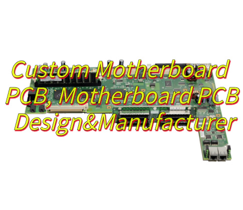
Are you looking to create a custom motherboard PCB that balances performance, reliability, and cost-effectiveness for your next project? In this comprehensive guide, we’ll explore the key considerations for designing and manufacturing custom motherboard PCBs, from layer optimization to material selection and thermal management.
At EBest Circuit (Best Technology), we’ve been delivering custom motherboard PCB solutions for over 20 years, combining advanced engineering expertise with state-of-the-art manufacturing capabilities. Our services include end-to-end support—from motherboard PCB design and prototyping to high-volume production. We specialize in multi-layer boards (up to 32 layers) and high-frequency applications, offering free DFM analysis to eliminate design flaws and reduce costs. With 24-hour expedited prototyping, ISO-certified quality control, and transparent pricing, we ensure your project stays on schedule and within budget. Feel free to contact us: sales@bestpcbs.com.
What Is Custom Motherboard PCB?
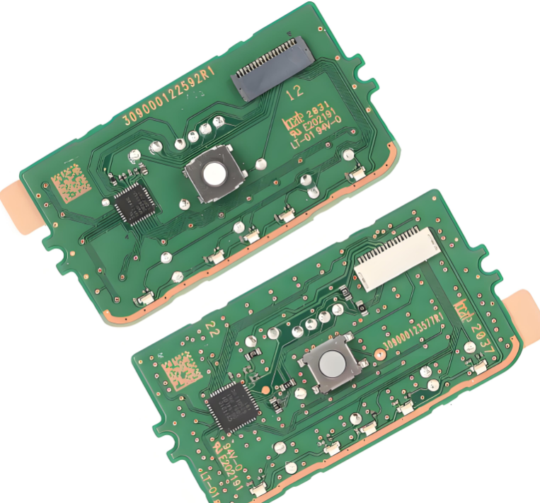
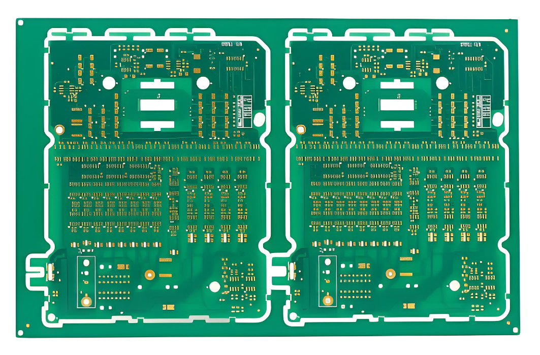
A custom motherboard PCB is a printed circuit board designed to meet specific functional, physical, and performance requirements for computing systems. Unlike generic motherboards, custom PCBs integrate unique features such as specialized connectors, power management modules, or high-speed signal paths. During assembly, these PCBs undergo a precise process where components like integrated circuits, resistors, and capacitors are soldered onto the board using surface mount technology (SMT) or through-hole technology. This meticulous assembly ensures that each custom motherboard PCB functions optimally, delivering the tailored performance that its design demands.
How to Custom the Layer Design of Motherboard PCB?
Layer design is critical for motherboard PCB design, as it directly impacts signal integrity, power efficiency, and manufacturability. Here’s a step-by-step approach:
- Route with Clearance: Maintain a minimum clearance of 8-10 mils between traces to avoid short circuits. Ensure that high-voltage traces have even greater separation to prevent arcing.
- Plan for Thermal Management: Incorporate thermal vias to efficiently transfer heat from power components to internal layers. Use thermal relief patterns around pads to prevent soldering issues caused by excessive heat.
- Design for Testability: Include test points on critical signals for easy access during manufacturing testing. Ensure test points are placed away from components to allow for automated test equipment (ATE) probing.
- Classify Signal Types: Separate high-speed signals (e.g., PCIe, USB) from low-speed signals (e.g., GPIO) to minimize crosstalk. Use dedicated ground planes between signal layers for isolation.
- Determine Layer Count: Start with a 4-layer stack-up (2 signal layers, 1 power plane, 1 ground plane) for basic designs. For complex systems, add layers for differential pairs or embedded components.
- Optimize Stack-up: Place analog and digital signals on separate layers to reduce EMI. Use symmetric layer structures to prevent warping during thermal cycling.
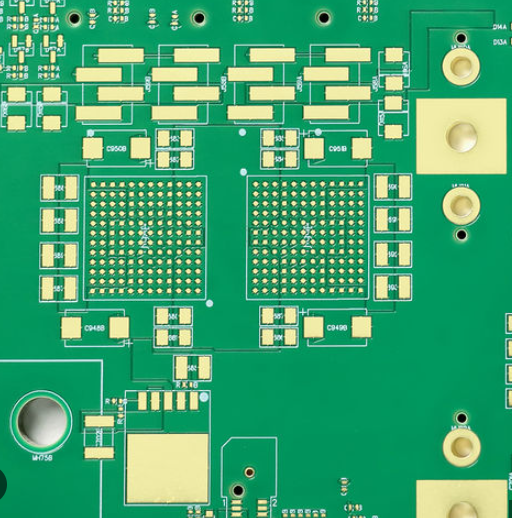
- Control Impedance: Calculate trace widths and dielectric thicknesses to achieve target impedance (e.g., 50Ω for USB 3.0). EBest Circuit (Best Technology) offers ±10% impedance tolerance for values >50Ω and ±5Ω for ≤50Ω .
- Manage Vias: Use buried or blind vias for HDI boards to reduce layer count. Ensure vias are spaced at least 12 mil apart to avoid copper cracking.
How to Select the Material of Custom Motherboard PCB?
Material choice influences thermal stability, electrical performance, and cost. Here’s a breakdown of common options:
- FR4: The industry standard for most motherboards, offering a balance of mechanical strength and thermal resistance (TG ~130–180°C). Ideal for consumer electronics.
- Rogers: High-frequency materials with low dielectric loss (Dk ~2.2–3.0), suitable for 5G, Wi-Fi, or RF applications.
- Metal-Core PCBs: Aluminum or copper substrates for enhanced heat dissipation, used in power-hungry components like GPUs.
- High-TG FR4: TG >180°C for automotive or industrial environments with extreme temperatures.
Consider factors like operating temperature, signal frequency, and budget. EBest Circuit (Best Technology) stocks materials from Rogers, Dupont, and other leading suppliers, ensuring compatibility with your design requirements.
How to Design Motherboard PCB Circuit Layout for Signal Integrity?
Signal integrity is paramount in motherboard PCB design, especially for high-speed interfaces. Follow these guidelines:
- Minimize Crosstalk: Route high-speed signals (e.g., clock lines) perpendicular to adjacent layers. Maintain trace spacing of at least 3x the trace width.
- Differential Pair Routing: Use matched-length pairs for USB, HDMI, or Ethernet to reduce EMI. Ensure impedance matching within ±10%.
- Ground Plane Continuity: Avoid splits in ground planes, as they disrupt signal return paths and increase noise. Use stitching vias to connect fragmented ground planes.
- Termination Techniques: Add series resistors or AC coupling capacitors to prevent signal reflections. For low-voltage differential signaling (LVDS), use parallel termination at the receiver.
- Layer Stack-up Optimization: Select appropriate dielectric materials with low loss tangent values and carefully balance the number of signal and power/ground layers to control impedance and reduce signal attenuation.
- Avoid Sharp Corners: Use rounded or 45-degree angles when routing traces instead of sharp 90-degree corners to minimize signal reflections and electromagnetic radiation.
- Power Plane Decoupling: Place decoupling capacitors close to the power pins of integrated circuits. Use a combination of different capacitor values (e.g., 0.1 μF and 10 μF) to cover a wide range of frequencies and reduce power supply noise.
- Signal Isolation: Separate sensitive analog signals from noisy digital signals by creating physical barriers or using dedicated layers and routing strategies to prevent interference.
How to Optimize PCB Motherboard Thermal Management Design?
Effective thermal management prevents component degradation and extends product lifespan. Implement these strategies:
- Copper Thickness: Use 2–3 oz copper for power planes to handle high currents. EBest Circuit (Best Technology) supports up to 30 oz copper for extreme applications.
- Heat Sink Integration: Design thermal vias under hot components (e.g., CPUs) to transfer heat to the chassis. Use thermal interface materials (TIMs) for better conductivity.
- Fan Placement: Position fans near high-power components, ensuring airflow paths avoid stagnant zones. Use CFD simulations to validate cooling efficiency.
- Thermal Relief Pads: Add relief pads around through-hole components to prevent solder joint fatigue from thermal expansion.
- Layer Stack-up Optimization: Incorporate additional internal copper layers dedicated to heat spreading, increasing the overall thermal conductivity of the PCB and enabling more efficient heat dissipation across the board.
- Component Layout Strategy: Group heat-generating components together in an area of the PCB with ample space for ventilation, separating them from heat-sensitive components to minimize thermal interference.
- Surface Finish Selection: Choose a surface finish with good thermal properties, such as immersion silver or electroless nickel immersion gold (ENIG), which can enhance heat transfer from components to the PCB surface.
- Vented Enclosure Design: If applicable, coordinate the PCB design with the enclosure, creating vents or openings that align with the natural airflow patterns on the board to allow hot air to escape and cool air to enter.
- Heat Pipe Incorporation: Integrate heat pipes into the PCB design for critical components. Heat pipes can rapidly transfer heat from high-temperature areas to cooler regions, effectively spreading heat across a larger surface area for improved cooling.
How to Choose A Trusted Custom Motherboard PCB Manufacturer?
Selecting the right manufacturer ensures your design is executed flawlessly. Look for:
- Technical Expertise: Experience in multi-layer PCB design, HDI, and high-frequency applications. EBest Circuit (Best Technology)’s 20+ engineers provide SI/PI analysis and DFM checks.
- Advanced Design Tools: Utilization of industry-standard software like Altium Designer, Or CAD, and PADS for precise and efficient PCB design.
- Material Options: Offering a wide range of PCB materials including FR-4, Rogers, and high TG laminates to suit different performance requirements.
- Certifications: ISO 9001, IATF 16949 for automotive/aerospace compliance.
- Prototyping Capabilities: Rapid turnaround (24–72 hours) for proof-of-concept testing.
- Flexible Prototyping: Support for both rigid (like FR4 PCB, MCPCB) and flexible PCB prototypes, enabling versatile product development.
- Quality Control: AOI, X-ray, and functional testing to ensure zero defects. EBest Circuit (Best Technology)’s 70+ quality checks include automated optical inspection and impedance testing.
- Traceability: Full traceability of materials and manufacturing processes for complete quality assurance.
- Transparent Communication: Real-time WIP updates and dedicated project managers.
- Customized Reporting: Providing detailed reports on design, manufacturing, and testing for clients’ records and analysis.
Can Your Manufacturer Support Custom Motherboard PCB Prototyping?
Yes. EBest Circuit (Best Technology) offers custom motherboard PCB prototyping with 24-hour expedited service for urgent projects. Our process includes:
- Design Review: Free DFM analysis to identify manufacturability issues.
- Material Selection: Access to FR4, Rogers, and other specialty materials.
- Rapid Fabrication: 2-layer boards in 24 hours, 4-layer in 48 hours, and 6–8-layer in 72 hours.
- Testing: Comprehensive electrical and mechanical tests to validate performance.
How Can We Deliver Custom Motherboard PCB Prototypes in 48-72 Hours?
To achieve 72-hour delivery, we:
- Prioritize Urgent Orders: Dedicated production lines for prototypes.
- Streamline Communication: Direct access to engineers for quick design adjustments.
- Pre-Approved Materials: Stocked inventory of common materials to eliminate delays.
- Express Shipping: Partner with DHL/FedEx for global delivery within 24–48 hours.
At EBest Circuit (Best Technology), we understand the importance of speed without compromising quality. Our prototyping services are backed by 18+ years of manufacturing experience and ISO-certified processes, ensuring your prototype meets or exceeds expectations.