

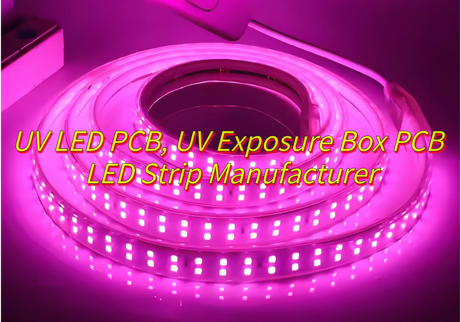
Looking for UV LED PCB solution? This guide includes UV LED PCB’s types, industrial uses, quality control methods, manufacturer selection criteria, and system integration approaches for precision manufacturing.
EBest Circuit (Best Technology) delivers UV LED PCB, especially for UV exposure box PCB LED strips optimized for industrial applications. The company employs advanced multi-lens optical arrays to achieve ±3% irradiance uniformity, ensuring consistent curing and photolithography results. With copper-clad FR4 substrates paired with precision thermal vias, thermal stability remains below 60℃ even during extended high-power operations. Custom-engineered solutions support 365nm and 405nm wavelengths, matched to specific photoresist requirements, while narrow-band filters enhance spectral purity. Modular designs allow hot-swappable replacements without system recalibration, minimizing downtime. Rigorous testing protocols include automated optical inspection and UV radiometer validation to guarantee <5% batch-to-batch energy density variance. IP67-rated environmental sealing protects components against harsh chemical exposure. The company provides rapid prototyping with 10-day lead times for sample approvals and scales production to 50,000+ units monthly. Technical teams offer application-specific guidance on beam alignment, PWM dimming configurations, and compliance with semiconductor safety standards. For UV LED strip solutions balancing precision, durability, and scalability, contact us today: sales@bestpcbs.com.
What Is UV LED PCB?
A UV LED PCB, or Ultraviolet Light-Emitting Diode Printed Circuit Board, is a specialized circuit board designed to support and power ultraviolet light-emitting diodes (UV LEDs) for applications requiring precise UV light emission. Constructed with a substrate (often FR-4 or metal-core laminates for heat dissipation), conductive traces for efficient energy flow, and solder pads for secure LED mounting, these boards prioritize thermal management, electrical efficiency, and UV resistance.
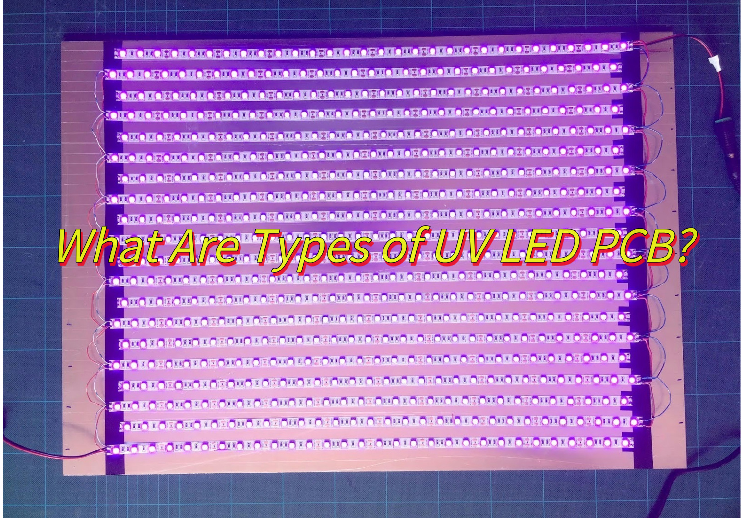
What Are Types of UV LED PCB?
UV LED PCBs are categorized based on wavelength ranges, packaging technologies, and structural designs, each tailored to optimize performance for specific applications. Below are the primary types:
1. Wavelength-Specific UV LED PCBs
- UVA (315–400 nm): Dominates industrial uses like curing adhesives, coatings, and UV inks. Common wavelengths include 365nm (ideal for surface curing) and 395nm (effective for deep-layer curing).
- UVB (280–315 nm): Primarily used in medical applications, such as 293nm UVB light therapy for skin conditions like psoriasis.
- UVC (200–280 nm): Focuses on sterilization, commonly found in 250–265nm UVC LED PCBs for disinfecting water, air, and surfaces in healthcare and consumer products.
2. Packaging Technology Variants
- COB (Chip-on-Board) UV LED PCBs: Integrate multiple LED chips directly onto the board for high-intensity output, suitable for large-area curing systems.
- SMD (Surface-Mounted Device) UV LED PCBs: Offer compact designs and easy automation, widely used in printers, exposure units, and consumer devices.
- DOB (Device-on-Board) UV LED PCBs: Combine LED arrays with drivers or controllers on a single board, streamlining integration into equipment like scanners or medical devices.
3. Material-Based Classifications
- Metal-Core PCBs (MCPCB): Use aluminum or copper substrates for enhanced heat dissipation, critical for high-power UV LEDs in curing or exposure systems.
- Ceramic PCBs: Provide superior thermal stability and UV resistance, ideal for harsh environments like industrial exposure boxes or aerospace applications.
- Flexible UV LED PCBs: Adopt polyimide substrates for bendable designs, enabling integration into irregularly shaped devices or wearable tech.
4. Application-Specific Types
- UV Exposure Box PCBs: Feature precise wavelength control and uniform light distribution for PCB fabrication, lithography, and 3D printing.
- UV Curing System PCBs: Optimize energy efficiency and thermal management for adhesive curing in electronics, automotive, and dental industries.
- UV Sterilization PCBs: Integrate UVC LEDs with smart sensors for portable disinfection devices, water purifiers, and HVAC systems.
What Are Application of UV LED PCBs?
Below are UV LED PCB’s applications:
Industrial Curing and Adhesive Bonding
- UV LED PCB Curing Systems: These boards power high-intensity UV lamps used to instantly cure adhesives, coatings, and inks in electronics, automotive, and optical manufacturing. Their energy efficiency reduces operating costs, while wavelength precision ensures flawless curing in seconds.
- PCB Manufacturing: UV LED PCB exposure systems transfer circuit patterns onto substrates with micron-level accuracy, critical for producing high-density PCBs and semiconductor components.
Printing and Packaging
- UV Inkjet Printing: UV LED PCB-driven systems cure inks on labels, packaging, and commercial prints, delivering vibrant colors and scratch-resistant finishes without solvents.
- 3D Printing: Enable rapid curing of resin-based materials, essential for industrial prototyping and dental applications.
Medical and Healthcare
- Sterilization Equipment: UV LED PCBs in UVC-powered devices disinfect medical tools, surfaces, and water supplies, offering chemical-free pathogen elimination.
- Diagnostic Tools: UV LED PCB scanners detect fluorescence in lab samples, aiding in disease diagnosis and genetic testing.
Quality Control and Inspection
- UV LED PCB Scanners: Used in anti-counterfeiting systems to identify hidden marks on currency, documents, and luxury goods. They also inspect UV-cured coatings for defects in electronics and automotive parts.
- Material Testing: UV exposure systems simulate sunlight degradation to evaluate the lifespan of plastics, coatings, and composites.
Automotive and Aerospace
- Adhesive Bonding: UV LED PCB curing secures lightweight components in electric vehicles and aircraft, reducing weight while maintaining structural integrity.
- Interior Lighting: Power UV-resistant LEDs for durable, low-energy cabin lighting.
Consumer Electronics
- Smartphone Assembly: UV LED PCBs cure protective coatings on screens and sensors, enhancing scratch resistance.
- Wearables: Enable compact UV sterilization modules in fitness trackers and smartwatches.
By integrating UV LED PCB curing, exposure systems, and scanners into these sectors, manufacturers achieve higher precision, lower energy consumption, and greater operational flexibility, solidifying UV LED PCBs as a cornerstone of modern technology.
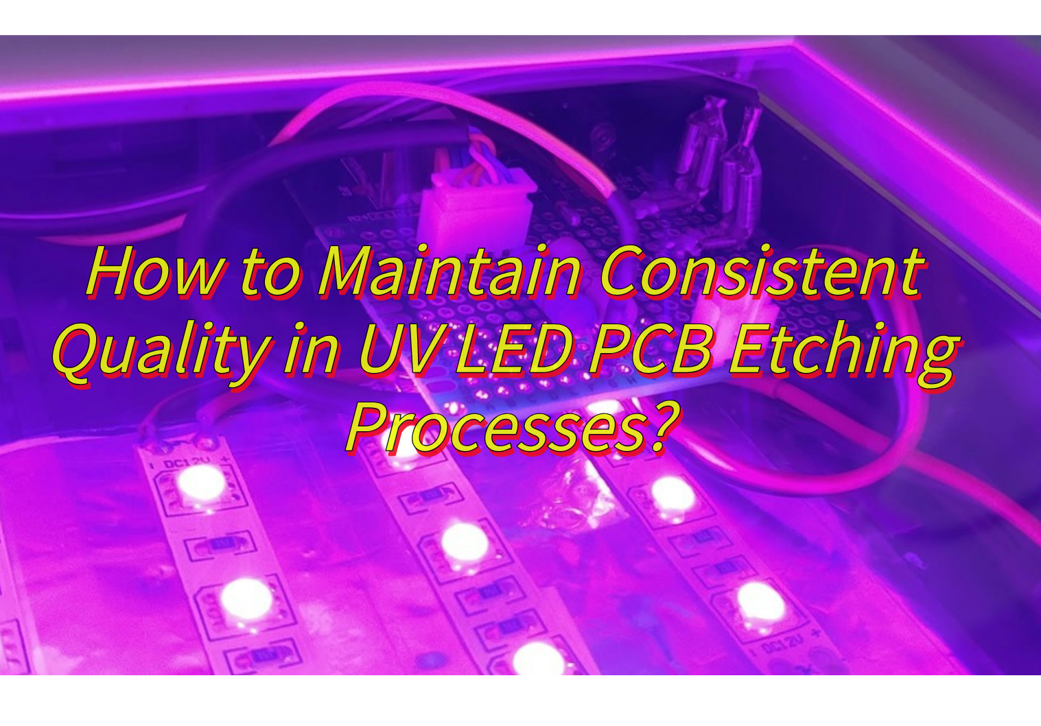
How to Maintain Consistent Quality in UV LED PCB Etching Processes?
Ensuring uniform quality in UV LED PCB etching demands rigorous process control, from material selection to final inspection. Below are proven strategies to minimize defects and optimize performance:
1. Optimize Etching Chemistry and Parameters
- Control etchant composition and temperature to prevent over-etching or residue. Use automated systems to monitor pH levels and adjust chemistry in real time.
- Set precise etching times based on copper thickness and desired trace resolution. Even minor deviations can disrupt patterns critical for UV LED PCB exposure systems.
2. Calibrate Equipment for Accuracy
- Align UV LED PCB exposure systems meticulously to ensure even pattern transfer. Misalignment causes uneven etching, leading to faulty circuits.
- Adjust spray pressure and conveyor speed in etching machines to guarantee uniform etchant distribution across the PCB surface.
3. Use High-Quality Resist Materials
- Select dry films compatible with UV LED wavelengths (e.g., 365nm or 395nm). Incompatible films may cure unevenly, causing resist peeling or incomplete etching.
- Store films in climate-controlled environments to prevent moisture absorption, which weakens adhesion and causes defects during etching.
4. Implement Real-Time Quality Checks
- Integrate UV LED PCB scanners into production lines to detect etching flaws like undercutting or residue. Immediate feedback allows instant adjustments to parameters.
- Use laser metrology tools to measure trace widths and spacing post-etching, ensuring compliance with design specifications.
5. Maintain Stable Environmental Conditions
- Control workshop humidity and temperature to prevent PCB warpage or uneven etchant evaporation. Fluctuations risk inconsistent etching results.
- Reduce airborne contaminants with laminar flow hoods or cleanroom zones, particularly during resist lamination and exposure.
6. Train Teams on Standardized Workflows
- Develop SOPs for equipment setup, resist application, and inspections. Consistent protocols minimize human error and variability.
- Educate operators on defect recognition, such as pinholes or over-etching, and how to troubleshoot using UV LED PCB scanners.
7. Conduct Pilot Runs for New Materials
- Test new etchants or films on sample PCBs before full-scale production. Use UV LED PCB exposure systems to simulate real-world conditions and validate compatibility.
- Document findings to refine processes and establish benchmarks for future batches.
How to Choose a UV Exposure Box PCB LED Strip Manufacturer?
Selecting the right UV exposure box PCB LED strip manufacturer requires careful evaluation of technical expertise, quality standards, and support capabilities. Below are factors to consider:
1. Technical Expertise and Customization
- Wavelength Range: Ensure the manufacturer offers UV LED strips in wavelengths like 365nm, 385nm, or 405nm to match your exposure box’s optical requirements.
- Uniformity and Precision: Verify if the LED strips provide consistent light output across their length, critical for even exposure in PCB fabrication.
- Customization Options: Choose a manufacturer that can tailor strip dimensions, LED density, and thermal management solutions to fit your exposure box design.
2. Quality Control and Certifications
- Material Standards: Confirm the use of high-grade PCB substrates (e.g., FR-4 or aluminum-core) and UV-resistant coatings to prevent degradation.
- Testing Protocols: Look for manufacturers with in-house testing for light decay, thermal stability, and wavelength consistency under prolonged UV exposure.
- Certifications: Prioritize companies with ISO 9001 or similar certifications, ensuring adherence to global quality benchmarks.
3. Performance and Durability
- Lifespan and Warranty: Select LED strips with a rated lifespan exceeding 20,000 hours and a warranty covering premature failures.
- Thermal Management: Ensure the manufacturer incorporates heat sinks or metal-core PCBs to dissipate heat efficiently, preventing performance drift.
4. Cost and Scalability
- Pricing Transparency: Request detailed quotes breaking down costs for materials, assembly, and testing to avoid hidden fees.
- MOQ Flexibility: Opt for manufacturers accommodating both small-batch prototypes and large-scale production runs.
- Supply Chain Reliability: Confirm the manufacturer has stable access to UV LED chips and components to avoid delays.
5. Customer Support and Documentation
- Technical Guidance: Choose a manufacturer offering support for integrating LED strips into your exposure box, including optical simulations if needed.
- Documentation: Ensure they provide datasheets with spectral graphs, thermal resistance data, and compliance certificates (e.g., RoHS).
6. Industry Reputation and Reviews
- Case Studies: Request examples of previous UV exposure box projects to gauge their expertise in your application domain.
- Client Feedback: Check online reviews or industry forums for insights into reliability, communication, and post-sales service.
How to Ensure Longevity of UV LED PCB Circuits in Harsh Environments?
UV LED PCBs are vital in applications like curing systems, medical devices, and industrial exposure units, but their performance can degrade in harsh conditions. Below are actionable steps to extend their lifespan:
1. Use High-Grade, Environment-Resistant Materials
- Opt for PCB substrates like FR-4 TG 170+ or ceramic composites to withstand high temperatures and thermal cycling without warping or delamination.
- Apply conformal coatings (e.g., epoxy or silicone) to shield against moisture, chemicals, and dust, which are common in industrial or outdoor settings.
2. Optimize Circuit Design for Thermal Management
- Increase copper trace widths to reduce electrical resistance and heat buildup, especially near LED nodes.
- Incorporate thermal vias under LEDs to dissipate heat into the PCB’s inner layers, preventing localized overheating.
- Avoid dense component clustering to ensure uniform airflow and cooling in enclosed or high-temperature environments.
3. Select UV-Resistant Components and Solder
- Use LED packages with silicone encapsulation instead of epoxy, as silicone resists yellowing and UV degradation over time.
- Choose solder paste formulations rated for high-temperature operation (e.g., SAC305) to prevent joint cracking under thermal stress.
4. Implement Robust Enclosure and Sealing
- House PCBs in IP65-rated enclosures to block moisture, oils, or particulates in environments like factories or outdoor installations.
- Use gaskets or potting compounds to seal gaps between connectors and enclosures, preventing ingress of contaminants.
5. Control Operating Conditions Proactively
- Limit duty cycles to prevent prolonged UV exposure, which accelerates material aging. Use intermittent operation where possible.
- Maintain ambient temperatures below 60°C using fans, heat sinks, or liquid cooling systems if operating in enclosed spaces.
6. Regularly Monitor and Maintain Performance
- Schedule periodic inspections to check for discoloration, delamination, or loose connections using thermal cameras or UV LED PCB scanners.
- Clean PCBs with isopropyl alcohol to remove residue buildup, which can block heat dissipation and cause hotspots.
7. Prioritize Power Supply Stability
- Use voltage regulators or surge protectors to shield against power fluctuations, which stress LEDs and reduce their lifespan.
- Implement soft-start circuits to minimize inrush currents during power-up, protecting LEDs from sudden thermal shocks.
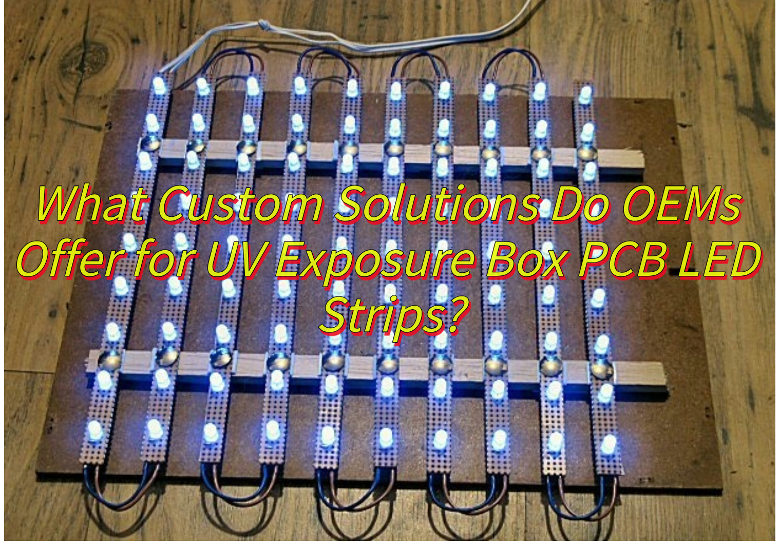
What Custom Solutions Do OEMs Offer for UV Exposure Box PCB LED Strips?
Original Equipment Manufacturers (OEMs) provide tailored solutions to optimize UV exposure box PCB LED strips for specific applications, environments, and performance demands. Below are the customization options they typically offer:
1. Wavelength and Spectral Output Adjustments
- Custom UV Wavelengths: OEMs can fine-tune LED strips to emit specific wavelengths (e.g., 365nm, 385nm, or 405nm) to match the optical requirements of your exposure process, ensuring precise curing or imaging.
- Spectral Bandwidth Control: Adjust the full width at half maximum (FWHM) of the UV output to enhance resolution in applications like semiconductor lithography or fine-line PCB etching.
2. Mechanical and Dimensional Customization
- Flexible or Rigid Form Factors: Design LED strips to fit unique exposure box geometries, including curved or narrow spaces, using flexible PCB substrates or ultra-thin rigid boards.
- Connector and Pinout Customization: Modify connector types, spacing, and orientation to streamline integration into existing or prototype exposure systems.
3. Thermal Management Enhancements
- Integrated Heat Sinks: Add aluminum or copper heat sinks directly onto the PCB to dissipate heat efficiently, preventing thermal degradation in high-power UV LEDs.
- Metal-Core PCBs (MCPCB): Use aluminum or copper-clad boards to improve thermal conductivity, critical for maintaining LED performance in continuous-use exposure boxes.
4. Optical and Light Distribution Upgrades
- Lens Arrays and Diffusers: Incorporate micro-lens arrays or diffusers to homogenize UV light output, reducing hotspots and ensuring even exposure across the PCB surface.
- Polarization Filters: Add linear or circular polarizers to minimize glare and improve contrast in optical inspection or photolithography applications.
5. Electrical and Control System Integration
- PWM Dimming and Control: Integrate pulse-width modulation (PWM) drivers to adjust UV intensity digitally, enabling precise energy control for different materials or layer thicknesses.
- Feedback Sensors: Embed temperature or light-output sensors for real-time monitoring, allowing automated adjustments to maintain consistency.
6. Environmental and Durability Upgrades
- Conformal Coatings: Apply epoxy, silicone, or parylene coatings to protect against moisture, chemicals, or abrasion in industrial or outdoor exposure boxes.
- IP Rating Enhancements: Seal LED strips to meet IP65, IP67, or higher ratings for dust and water resistance, extending lifespan in harsh environments.
7. Performance and Lifetime Optimization
- High-Efficiency LED Binning: Select LEDs from tighter binning ranges to ensure uniform brightness and color temperature across strips, critical for multi-LED exposure systems.
- Accelerated Aging Tests: Pre-test LED strips under simulated operating conditions to guarantee performance and lifespan expectations.
How to Integrate UV LED Strip PCBs into Exposure Box Systems for Precision Applications?
Integrating UV LED strip PCBs into exposure box systems demands precision engineering to ensure consistent performance, uniform light distribution, and long-term reliability. Below are actionable steps to achieve optimal results:
1. Define System Requirements
- Wavelength and Intensity: Determine the exact UV wavelength (e.g., 365nm, 385nm) and irradiance (mW/cm²) required for your application, such as PCB etching or photolithography.
- Uniformity Targets: Set acceptable tolerances for light uniformity (e.g., ±3% variation) to guarantee consistent exposure across the entire work area.
2. Customize LED Strip Layout and Optics
- LED Density and Spacing: Arrange LEDs in dense grids for high-resolution tasks or staggered patterns to balance coverage and cost.
- Optical Enhancements: Integrate collimating lenses or engineered diffusers to shape light output, minimizing hotspots and ensuring edge-to-edge consistency.
- Polarization Control: Add linear polarizers to reduce glare in optical inspection or imaging applications.
3. Optimize Thermal Management
- Heat Sink Design: Customize aluminum or copper heat sinks with fins or vapor chambers to dissipate heat from high-power LEDs efficiently.
- Active Cooling: Install fans, blowers, or liquid cooling systems if the exposure box operates in ambient temperatures exceeding 25°C.
- Thermal Interface Materials: Use high-conductivity pads or pastes between LED strips and heat sinks to eliminate air gaps and improve heat transfer.
4. Electrical and Control System Integration
- PWM Dimming: Implement pulse-width modulation (PWM) drivers to adjust UV intensity in 1% increments, enabling precise exposure control for varying materials.
- Feedback Sensors: Embed thermistors or photodiodes to monitor real-time temperature and light output, triggering alerts if deviations occur.
- Safety Interlocks: Design circuits to shut down LEDs automatically if overheating, door breaches, or power surges are detected.
5. Mechanical and Environmental Customization
- Form Factor Adaptation: Modify strip length, width, and flexibility to fit proprietary exposure box geometries, including curved or modular designs.
- Sealing and IP Rating: Seal strips with epoxy or silicone gaskets to achieve IP65/IP67 ratings, protecting against dust, moisture, or chemicals in industrial settings.
- Vibration Damping: Use anti-vibration mounts or foam inserts if the exposure box is deployed in high-shock environments (e.g., factory floors).
6. Pre-Integration Testing and Calibration
- Optical Bench Testing: Validate light uniformity, wavelength accuracy, and intensity using spectroradiometers and integrating spheres before installation.
- Aging Tests: Stress-test LED strips under simulated operating conditions to identify and resolve premature failure modes.
- Mapping and Compensation: Use UV LED PCB scanners to create irradiance maps of the exposure area, then adjust LED drivers to correct for minor inconsistencies.
7. Software and Automation Integration
- API Development: Create software interfaces to control exposure time, intensity, and wavelength directly from lab automation or manufacturing execution systems (MES).
- Recipe Storage: Save exposure parameters (e.g., duration, dimming profiles) as digital recipes for repeatable, audit-ready results.
- Remote Diagnostics: Enable remote monitoring of LED health, temperature, and performance metrics via IoT-compatible controllers or cloud platforms.
In conclusion, that’s all about UV LED PCB’s types, industrial uses, quality control methods, manufacturer selection criteria, and system integration approaches for precision manufacturing. If you want to know more about UV LED PCB, welcome to leave a message below this blog. Looking forward to your message!
Tags: UV Exposure Box PCB LED Strip Manufacturer, UV LED PCB