

Since 2006, EBest Circuit (Best Technology) has specialized in metal core PCB & PCB board manufacturing services, with our headquarters located in Shenzhen, China, serving as the heart of our global operations. To enhance our global reach, we’ve also established SMT factories in both China and Vietnam, to offer an efficient support for customers worldwide. Our facility holds several industry certifications, including ISO9001, ISO13485, IATF16949, and AS9100D, reflecting our commitment to high-quality standards across all sectors we serve.
Additionally, EBest Circuit (Best Technology) utilizes the MES Material Traceability System, which enables full traceability of every component, from incoming material inspection to final production. All components we use are UL, REACH, and RoHS certified, adhering to the highest global safety and environmental standards.
What is a Metal Core PCB?
A Metal Core PCB (MCPCB) is a type of printed circuit board that utilizes a metal substrate instead of traditional fiberglass or plastic materials. The main function of a metal core PCB is to provide higher thermal conductivity, which is especially beneficial in applications requiring efficient heat dissipation like LED lights. In a typical PCB, heat can accumulate and negatively affect the performance and lifespan of electronic components. However, the metal core serves as an effective medium for channeling heat away from sensitive areas, optimize the operation and longevity of the circuit.
Metal core PCBs are made with materials like aluminum or copper that allow for effective thermal transfer. They are primarily used in high-power applications, where managing heat is crucial to maintaining the functionality of devices.
What is MCPCB Core Made of?
The core of a Metal Core PCB is typically composed of a metal material that has superior thermal conductivity properties. The most commonly used metals are aluminum and copper, with aluminum being the most popular due to its cost-effectiveness and excellent thermal performance.
- Aluminum: Aluminum is often the metal of choice for MCPCB cores because it offers a combination of high thermal conductivity, light weight, and affordability. Its relatively low cost compared to copper makes it an attractive option for mass production, especially in consumer electronics and lighting applications.
- Copper: Copper has a higher thermal conductivity than aluminum and is typically used in more demanding applications that require superior heat dissipation. It is particularly useful in industries like telecommunications and automotive, where components generate significant amounts of heat and need to be efficiently managed.
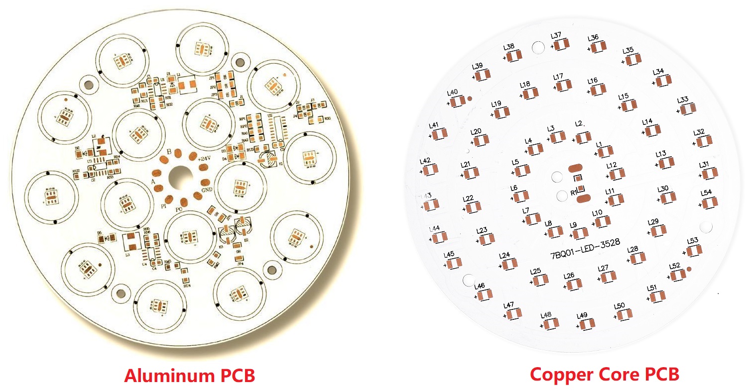
Aluminum Core PCB vs. Copper Core PCB
When deciding between an aluminum core PCB and a copper core PCB, it’s essential to consider the specific requirements of the application. Both types of metal core PCBs offer excellent thermal management, but there are differences in performance, cost, and suitability for various environments.
| Factor | Aluminum Core PCB | Copper Core PCB |
| Thermal Conductivity | Good thermal conductivity (about 170 W/m·K) | Excellent thermal conductivity (about 400 W/m·K) |
| Weight | Lightweight, ideal for portable devices | Heavier, more suitable for heavy-duty applications |
| Cost | Generally more cost-effective | More expensive due to the cost of copper |
| Thermal Management | Suitable for almost heat dissipation needs | Best for high power and extreme heat dissipation |
| Mechanical Strength | Moderate strength, suitable for most applications | High mechanical strength, suitable for demanding applications |
| Electrical Conductivity | Good, but not as high as copper | Superior electrical conductivity, ideal for high-performance circuits |
| Durability | Durable, but can corrode in harsh environments if not properly protected | Extremely durable and resistant to corrosion, making it ideal for rugged environments |
| Applications | Used in LED lighting, automotive, consumer electronics, and power supplies | Preferred in high-power electronics, RF applications, and high-end telecommunications |
| Heat Dissipation Efficiency | Adequate for most applications, but limited in extreme conditions | Optimal for high-performance applications that require rapid heat dissipation |
| Manufacturing Complexity | Easier to manufacture and more cost-effective for mass production | More complex and costly to manufacture, but necessary for high-heat applications |
What Are the Materials Used in Metal Core PCB?
The materials used in Metal Core PCBs are carefully selected to ensure high performance and reliability. The primary materials include:
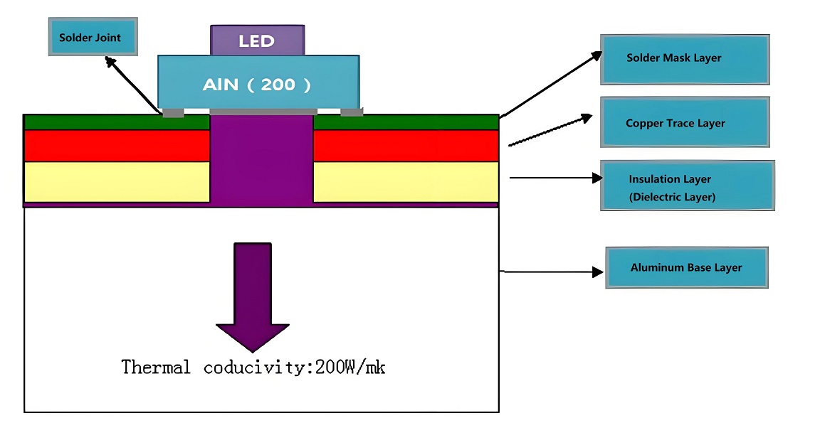
- Base Material (Metal Core): As mentioned earlier, the core of the PCB is typically made of aluminum or copper. The choice of metal directly impacts the thermal conductivity and cost-effectiveness of the PCB.
- Insulating Layer: Above the metal core, there is an insulating layer that electrically isolates the metal core from the copper traces on the PCB. This layer is typically made from a thermally conductive dielectric material, such as epoxy resin or fiberglass. The insulating layer ensures that the metal core doesn’t short-circuit the copper traces while still allowing for efficient heat transfer.
- Copper Foil: The copper foil is used to create the circuit traces. Copper is chosen for its excellent electrical conductivity and reliability. The copper is etched to form the required circuit pattern, allowing electrical signals to flow seamlessly through the PCB.
- Solder Mask: The solder mask is a protective layer that covers the copper traces to prevent oxidation and improve durability. It also provides electrical insulation to prevent short circuits and ensures that components are properly soldered.
- Silkscreen Layer: The silkscreen layer is used to print labels, markings, and other necessary information onto the surface of the PCB. This layer aids in component placement during assembly and provides identification for troubleshooting.
Together, these materials form a Metal Core PCB that is capable of efficiently managing heat while ensuring electrical performance and durability.
How Thick is a Metal Core PCB?
The thickness of a Metal Core PCB depends on various factors, including the application’s thermal and mechanical requirements. Typically, the total thickness of a metal core PCB ranges from 1.6 mm to 3.2 mm, but it can vary depending on the design and intended use.
- Core Thickness: The metal core itself typically ranges from 0.3 mm to 2.0 mm in thickness. Thicker cores provide better heat dissipation but may increase the overall cost of the PCB.
- Overall PCB Thickness: The overall thickness, including the copper traces, insulating layer, and solder mask, can vary depending on the complexity of the design and the type of components being used. For high-power applications, a thicker PCB may be necessary to ensure adequate heat management and mechanical strength.
How is a PCB Manufactured Step by Step?
The manufacturing of a Metal Core PCB (MCPCB) is a highly specialized process that involves several crucial steps to ensure thermal efficiency, reliability, and electrical performance. Below is a detailed breakdown of each step involved in the MCPCB manufacturing process.
1. Design and Layout Preparation
The first step in the manufacturing of an MCPCB is the design phase. Engineers and designers create the PCB layout, including the placement of components, traces, vias, and pads. This layout must consider factors like thermal management, electrical conductivity, and mechanical strength. The design is usually done using specialized software like AutoCAD or Altium Designer.
In the case of MCPCBs, the layout also includes specific considerations for the metal core, insulating layer, and the heat dissipation needs of the application. The thermal conductivity of the material, as well as the required heat dissipation paths, are factored into the design.
2. Core Material Selection
The next step involves selecting the appropriate core material. For MCPCBs, the core is typically made from metal, usually aluminum or copper. The choice of metal affects both the thermal performance and cost of the PCB.
Aluminum is lightweight, cost-effective while copper has superior thermal conductivity compared to aluminum, and is often used in more demanding applications that require exceptional heat dissipation, such as high-power electronics or automotive applications.
3. Insulating Layer Preparation
Next, an insulating dielectric material is applied to the metal core. This insulating layer is crucial for electrically isolating the metal from the copper traces while still enabling efficient heat transfer. The material used for this layer is typically a thermally conductive resin or fiberglass composite.
The insulating layer’s thickness depends on the requirements of the circuit. It must be thick enough to provide electrical isolation, yet thin enough to allow heat to pass through it efficiently. This layer is typically applied as a thin film or laminate and is then bonded to the metal core using heat and pressure.
4. Copper Foil Lamination
Once the insulating layer is in place, a layer of copper foil is laminated onto the surface. The copper foil is typically bonded to the insulating layer under high pressure and temperature.
Thicker copper foils are used for high-power applications, while thinner foils are sufficient for low-power circuits.
5. Circuit Etching
After the copper foil has been applied, the next step is to etch the circuit pattern. This is done using a chemical etching process, where the unwanted copper is dissolved away, leaving only the copper traces that form the electrical pathways.
The process including apply a photoresist film onto the copper, and then it is exposed to UV light through a mask. The board is then exposed to a chemical solution that etches away the exposed copper, leaving behind the desired circuit pattern.
6. Drilling and Plating
Once the copper traces have been etched, the next step is to drill holes for vias and component leads. Vias are used to establish electrical connections between different layers of the PCB, if applicable. Drilling is done with precision machinery to ensure the holes are accurately positioned.
After drilling, the holes are plated with copper to create electrical connections. The plating process involves depositing a thin layer of copper onto the walls of the drilled holes using an electroplating process. This creates the necessary conductive pathways for signals to travel through the different layers of the PCB.
7. Solder Mask Application
Next, a solder mask is applied to the PCB. The solder mask is a protective layer that prevents oxidation, protects the copper traces from damage. The solder mask is typically a green-colored epoxy-based material, although other colors can be used depending on the customer’s requirements, like red, black, white. Metal core PCB always use white solder mask to gather a good light reflection.
8. Silkscreen Printing
After the solder mask is applied, a silkscreen layer is used to print component labels, markings, and other important information on the surface of the PCB. This is helpful during assembly, as it indicates the proper locations for components to be placed.
The silkscreen printing is typically done using a screen printing process, where ink is pushed through a mesh screen to form the desired markings. Generally, the white solder mask with a black silkscreen, and black solder mask with a white silkscreen.
9. Inspection and Testing
Once the MCPCB has undergone the necessary manufacturing steps, it is thoroughly inspected for defects and tested for functionality. The metal core PCB always must pass three inspection – electrical, thermal, and mechanical requirements.
10. Final Assembly
The final step in the MCPCB manufacturing process is the assembly of electronic components onto the PCB. This involves placing components like resistors, capacitors, LEDs, and other active and passive elements onto the board and soldering them in place.
Component placement is typically done using automated machinery to ensure accuracy and speed. Once the components are placed, they are soldered onto the pads using either wave soldering or hand soldering, depending on the complexity of the design.
11. Quality Control and Shipping
Once the assembly is complete, the final MCPCB undergoes a final functional inspection and quality control check to ensure that it meets the required specifications. The finished product is then packaged and prepared for shipping to customers.
During the quality control phase, the board is examined for any signs of poor soldering, component misplacement, or other issues. If the board passes all inspections, it is ready for shipment.
Metal Core PCB Applications
Metal Core PCBs are used in a variety of industries, thanks to their exceptional thermal management capabilities. Common applications include:
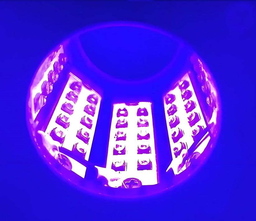
- LED lighting like pool lighting, UV led, led car lighting, high bay light, stair light, etc.
- Power supplies
- Automotive
- Sensors
- Electronic control units
- Telecommunications
- Consumer Electronics
- Computers
- Smartphones
- Televisions
FAQs
1. Can I design the dielectric layer much thinner on MCPCB?
Yes you can. Thinner dielectric layer has better thermal conductivity, but also has a lower breakdown voltage
2. Can you do gold immersion finish on double sided MCPCBs?
Yes, we can do gold immersion finish on double sided MCPCB, but the price will be less competitive than HASL-LF.
3. Top 6 factors affecting the final cost of MCPCB?
1) Board Dimention: For the non-rectangular board, we will calculate the longest two sides, for example, the circle is calculated according to the diameter.
2) Cu Thickness: The cost will be more expensive if the copper is thicker. We can provide 0.5 OZ, 1.0 OZ, 2.0 OZ, 3.0 OZ, up to 8 OZ.
3) Thermal Conductivity: The higher the thermal conductivity is, the more expensive the price is. At present, the highest thermal conductivity we can provide is 3W/m.K
4) Surface Finishing: The common Surface Finishing for MCPCB is HASL_LF, OSP ENIG (The normal thickness of gold is 1u”). ENIG is more expensive since the finished color is better than other surface Finishing, and it’s easier for components to solder and less prone to oxidation reaction.
5) Board Thickness: The commonly used thickness is 1.6mm+/-10%, and the thickest we have ever made is 4.0mm+/-10%. The price over 2mm or less than 1mm will be slightly expensive.
6) Soldermask: White / Black / Blue / Green / Red Oil (The Taiyo Soldermask is more expensive than normal, the advantage is the reflectivity will be better, which is suitable for LED board.)
7) Stack up/Construction: The more complex the structure, the more expensive the price, which is mainly executed on your requirements.
4. Which dielectric layer is recommended for LED (90+W) lighting?
If it is used for watt more than 90W, considering that the LED power is high, 3W.m.k or 2W/m.k is better than 1W/m.k.
5. What is Conformal coating of metal core PCB?
Conformal coating is a specially coating used to protect circuit boards and related equipment from environmental damage. it has good high and low temperature resistance, it can insulation, avoid moisture, leakage, shock, dust and so on.
Tags: mcpcb manufacture process, metal core pcb manufactuing process