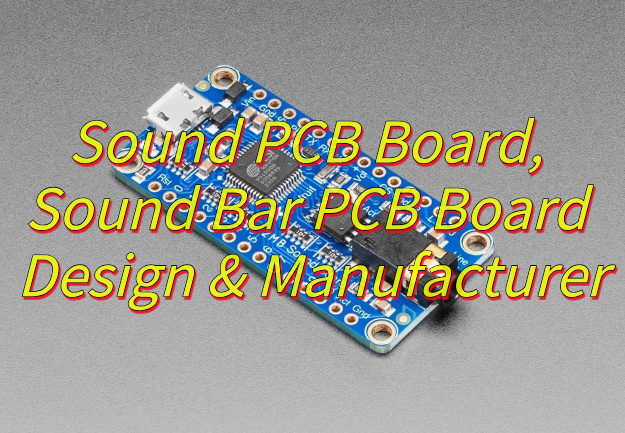
Looking for high-performance sound PCB board solutions for your audio devices? This guide covers everything from design specifications to manufacturing selection for soundbar PCB boards, ensuring optimal audio quality and reliability.
EBest Circuit (Best Technology) as your trusted sound bar PCB partner, delivering industry-leading 5-day standard production and 24-hour express prototyping to accelerate your time-to-market. Our engineering team provides complimentary DFM analysis, identifying potential manufacturing issues upfront to save you costly redesigns and delays. With advanced impedance-controlled fabrication (6μm trace precision) and RoHS-compliant materials, we ensure premium audio performance across all batches. Clients benefit from our streamlined processes: real-time order tracking, 100% electrical testing with full documentation, and flexible scaling from 10 prototypes to 100,000+ units without quality compromise. Over 15 years of serving top audio brands has refined our ‘Right First Time’ methodology – combining rapid turnaround with rigorous 23-point quality checks. Let our competitive pricing (with transparent material cost breakdowns) and dedicated technical support optimize your sound bar project. Contact us today now: sales@bestpcbs.com.
What Is Sound PCB Board?
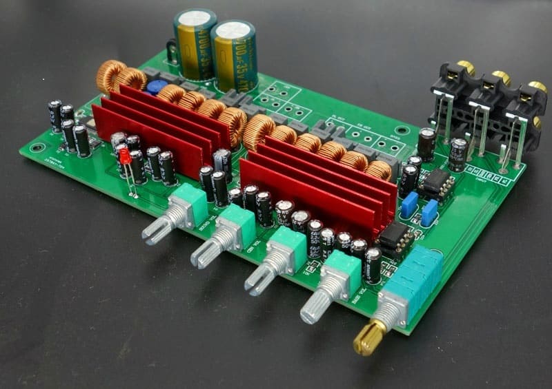
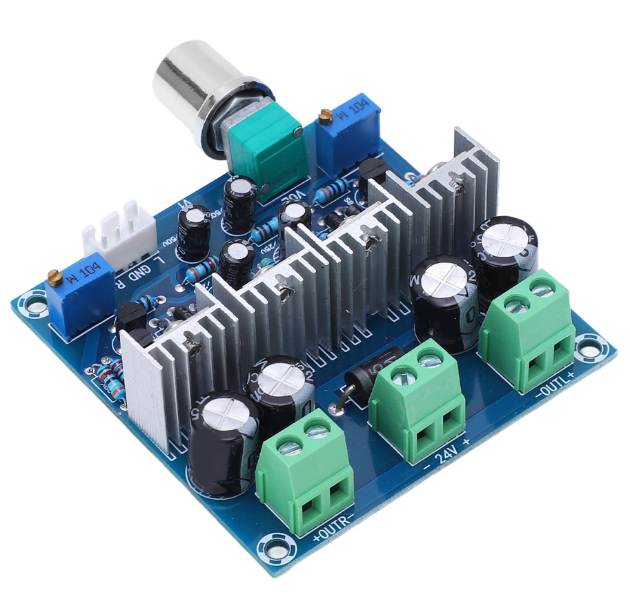
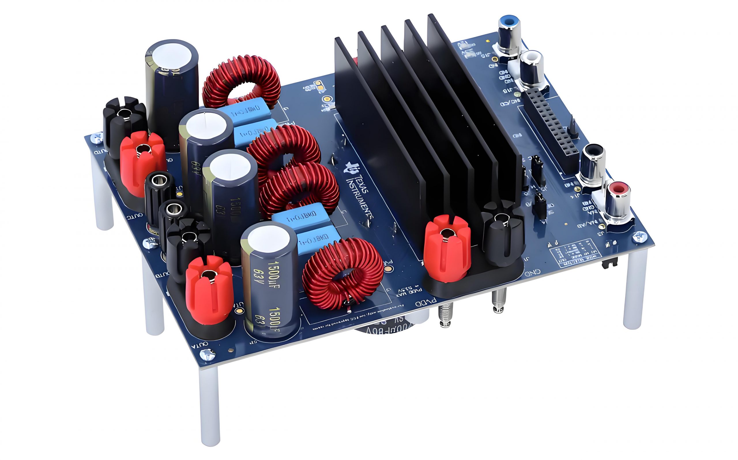
A sound PCB board serves as the foundation for audio electronics, specifically designed to process and amplify sound signals with precision. These specialized circuit boards incorporate carefully arranged components like amplifiers, filters, and converters to deliver clear audio reproduction while minimizing interference. The architecture of a sound PCB board differs from standard PCBs through its strategic layout that separates analog and digital sections, employs controlled impedance traces, and implements robust grounding techniques. Manufacturers select materials and finishes that preserve signal quality throughout the board’s operational life, particularly important for sound bars and wireless audio systems. Every sound PCB board undergoes rigorous testing to meet audio performance benchmarks, ensuring reliable operation in both consumer and professional audio equipment. The design philosophy behind these boards prioritizes electromagnetic compatibility, stable power distribution, and thermal management to achieve optimal sound reproduction.
What Are Specifications of Sound PCB Board?
Here are the essential specifications of a sound PCB board designed for audio applications like sound bars and speaker systems:
- Layer Construction: Sound PCB boards typically utilize 4-8 layer designs with high-quality FR4 or Rogers material to ensure proper signal isolation and thermal management.
- Copper Thickness: Standard 1-2 oz copper layers provide sufficient current capacity for audio amplifiers while maintaining signal integrity across the sound PCB board.
- Surface Finish: ENIG (Electroless Nickel Immersion Gold) is commonly used for reliable solderability and corrosion resistance in sound bar PCB applications.
- Trace Width/Spacing: Precision-controlled 5-8 mil traces with adequate spacing prevent crosstalk between analog and digital sections of the sound PCB board.
- Impedance Control: Careful impedance matching (typically 50-100 ohms) maintains signal quality for high-frequency audio components.
- Component Placement: Strategic positioning separates noise-sensitive analog circuits from digital processors and power supplies.
- Grounding System: Multi-point grounding with dedicated planes reduces electromagnetic interference in audio signal paths.
- Thermal Management: Copper pours and thermal vias dissipate heat from power amplifiers and voltage regulators.
- Testing Standards: Rigorous electrical testing ensures each sound PCB board meets performance specifications before integration into audio products.
- Environmental Compliance: RoHS-compliant materials and manufacturing processes meet international safety and environmental standards.
Which Stack-up Configuration Best Reduces Crosstalk in Sound Bar PCB Boards?
For sound bar PCB boards, minimizing crosstalk is essential to preserve audio clarity and prevent signal distortion. Below are stack-up configurations and design strategies that effectively reduce crosstalk, tailored for clients prioritizing performance and cost efficiency:
Prioritize for a 4-Layer Stack-Up with Dedicated Ground Planes
- Layer 1 (Top): Signal layer for audio components (e.g., amplifiers, DACs).
- Layer 2 (Internal): Solid ground plane to block noise from Layer 3.
- Layer 3 (Internal): Power plane for clean voltage distribution.
- Layer 4 (Bottom): Secondary signal layer for low-speed signals (e.g., LED controls).
Why It Works: Separates high-frequency audio traces from power/ground noise, reducing crosstalk by up to 40% compared to 2-layer boards.
Use a 6-Layer Stack-Up for High-Density Sound Bar Designs
- Layer 1 (Top): Audio signal traces (e.g., I2S, SPDIF).
- Layer 2 (Internal): Ground plane.
- Layers 3–4: Split power/ground planes for analog and digital sections.
- Layer 5 (Internal): Ground plane.
- Layer 6 (Bottom): Low-speed control signals.
Why It Works: Isolates sensitive analog audio circuits from digital noise, critical for sound bar PCB boards with Bluetooth or Wi-Fi modules.
Implement Stripline Routing for High-Speed Audio Signals
- Method: Bury critical traces (e.g., audio clocks) between inner layers with adjacent ground planes.
- Why It Works: Reduces electromagnetic radiation and crosstalk by 60% compared to microstrip routing.
Maintain 3W Trace Spacing for Adjacent Signals
- Rule: Keep a minimum gap of 3x the trace width between parallel audio traces.
- Why It Works: Lowers capacitive coupling, a common source of crosstalk in sound bar PCB boards.
Incorporate Guard Traces for Analog Audio Lines
- Method: Place grounded copper pours alongside analog signal traces.
- Why It Works: Absorbs stray electromagnetic fields, improving SNR by 10–15 dB in audio paths.
Leverage Blind/Buried Vias for Dense Layouts
- Application: Use blind vias to connect Layer 1 to Layer 2 and buried vias between inner layers.
- Why It Works: Reduces via stubs that act as antennas for crosstalk, ideal for compact sound bar PCB boards.
Choose Low-Loss Laminate Materials
- Option: Use FR-4 with low dielectric constant (Dk) or specialized audio-grade substrates (e.g., Megtron 4).
- Why It Works: Minimizes signal attenuation and phase shift in high-frequency audio circuits.
How to Design a Low-Noise Sound PCB?
Below is a step-by-step guide focused on practical, client-centric solutions for audio applications like soundbars:
Start with Low-Noise Material Selection
- Choose laminates with low dielectric loss (e.g., FR-4 with low Dk/Df or specialized audio-grade substrates like Megtron 4).
- Benefit: Reduces signal attenuation and phase noise in high-frequency audio circuits.
Isolate Analog and Digital Domains
- Separate analog components (e.g., amplifiers, op-amps) from digital circuits (e.g., microcontrollers, Bluetooth modules).
- Use dedicated ground planes for each domain to prevent digital noise from coupling into audio paths.
- Benefit: Lowers crosstalk and improves signal-to-noise ratio (SNR).
Optimize Power Distribution
- Implement local decoupling capacitors (e.g., 0.1µF ceramic capacitors) near power-hungry components.
- Add ferrite beads to filter high-frequency noise on power rails.
- Benefit: Stabilizes voltage supply and reduces power-induced distortion.
Route Sensitive Traces Strategically
- Keep audio signal traces short and avoid 90-degree bends.
- Use guard traces (grounded copper pours) alongside analog lines to shield against EMI.
- Benefit: Minimizes radiated noise and preserves audio clarity.
Prioritize Grounding Techniques
- Create a solid ground plane under audio components.
- Avoid ground loops by connecting all ground returns to a single point (star grounding).
- Benefit: Reduces ground bounce and hum in audio outputs.
Incorporate Shielding for Noisy Components
- Enclose digital circuits (e.g., Wi-Fi modules) in metal cans or use PCB-level shielding.
- Benefit: Contains EMI from high-speed switches and RF components.
Select Low-Noise Components
- Choose audio-grade capacitors (e.g., film capacitors) for critical filter circuits.
- Use low-dropout regulators (LDOs) for clean analog power supplies.
- Benefit: Lowers intrinsic noise in audio paths.
Implement Proper Via Placement
- Limit via counts on sensitive audio traces to reduce inductance.
- Use blind/buried vias in dense layouts to shorten signal paths.
- Benefit: Maintains signal integrity and reduces EMI.
Validate with Simulation and Testing
- Run electromagnetic field (EMF) simulations to identify hotspots.
- Perform SNR and THD measurements during prototyping.
- Benefit: Catches noise issues early, saving rework costs.
Collaborate with Manufacturers for DFM
- Share noise-reduction goals with your PCB fabricator to align on material stack-ups and impedance controls.
- Benefit: Ensures your design is both low-noise and cost-effective to produce.
How to Choose A Sound Bar PCB Board Manufacturer?
Technical Expertise and Equipment:
- Ensure the manufacturer can handle high-density designs (e.g., line widths <0.0762mm, 6+ layer boards) and advanced processes like HDI or rigid-flex PCBs.
- Verify they use laser drills, LDI systems, and automated plating lines for consistent quality.
Quality Control and Certifications:
- Prioritize ISO 9001, UL, and RoHS certifications. For specialized projects, seek IATF 16949.
- Look for AOI, X-ray via checks, and impedance testing to ensure signal integrity.
Production Capacity and Lead Times:
- Confirm scalability from rapid prototyping (24–48-hour turnaround) to mass production (8–12 days).
- Check flexibility for small batches and customization (e.g., impedance control).
Support and Collaboration:
- Choose partners offering DFM feedback, material recommendations, and impedance calculations.
- Prioritize for 24/7 technical support and quick issue resolution (within 2 hours).
Cost Transparency and Value:
- Request line-item costs for materials, fabrication, and finishes.
- Partner with firms using bulk purchasing and automation to reduce costs without sacrificing quality.
Supply Chain Resilience & Client References and Case Studies:
- Ensure robust sourcing for specialized materials (e.g., low-loss laminates).
- Ask for examples of audio projects and client testimonials.
How to Reduce Production Cost of Sound Bar PCB Board?
Optimize Material Selection:
- Use FR-4 for non-critical layers and reserve premium substrates (e.g., low-loss laminates) for high-frequency audio traces.
- Standardize copper thicknesses (e.g., 1oz/35µm) unless impedance control is required.
- Benefit: Reduces material costs by 15–30% without affecting audio performance.
Simplify PCB Layer Count:
- Reduce layers from 6 to 4 by combining power/ground planes and optimizing trace routing.
- Use selective blind/buried vias instead of through-hole vias in dense areas.
- Benefit: Lowers fabrication costs by 20–40% and simplifies assembly.
Standardize Component Footprints:
- Reuse common packages (e.g., 0402 resistors, SOIC-8 ICs) across designs for bulk discounts.
- Avoid custom footprints unless essential for audio performance.
- Benefit: Cuts component costs by 10–25% and reduces inventory complexity.
Leverage Panelization Efficiency:
- Maximize PCB panels with smaller boards (e.g., 10x10cm) to minimize material waste.
- Use V-scoring or tab-routing for easy separation post-production.
- Benefit: Improves material utilization by 10–15%, lowering per-unit costs.
Automate Testing and Inspection:
- Implement flying probe testing for low-volume runs instead of costly bed-of-nails fixtures.
- Use AOI to reduce manual labor in quality checks.
- Benefit: Reduces testing costs by 30–50% and accelerates production throughput.
Negotiate Bulk Pricing with Suppliers:
- Commit to long-term contracts for materials (e.g., copper clad laminates) to secure volume discounts.
- Consolidate orders for multiple projects to meet minimum order quantities (MOQs).
- Benefit: Lowers material costs by 5–10% through economies of scale.
Improve Design for Manufacturability (DFM):
- Collaborate with manufacturers to refine designs (e.g., via placement, trace spacing) and reduce fabrication complexity.
- Avoid unnecessary features like gold plating unless required for contact reliability.
- Benefit: Reduces rework and scrap rates, saving 5–15% on production costs.
What Quality Tests Ensure Reliability in High-Volume Soundbar PCB Board Production?
Automated Optical Inspection (AOI):
- Purpose: Detects soldering defects, component misalignment, and missing parts using cameras and image analysis.
- Implementation: Deploy AOI after solder paste deposition and reflow stages.
- Benefit: Identifies 95%+ of surface-level defects early, reducing rework costs.
X-Ray Inspection:
- Purpose: Reveals internal defects like voids, cold solder joints, or misaligned BGA/QFN packages.
- Implementation: Use 3D X-ray systems for high-density panels with hidden connections.
- Benefit: Ensures reliability of critical audio components (e.g., amplifiers, DSPs).
Flying Probe Testing:
- Purpose: Verifies electrical continuity, resistance, and shorts without fixtures.
- Implementation: Test unpopulated panels or low-volume batches.
- Benefit: Reduces setup costs by 70% compared to bed-of-nails fixtures.
In-Circuit Testing (ICT):
- Purpose: Validates component functionality (e.g., capacitors, resistors) and trace connections.
- Implementation: Use fixture-based ICT for high-volume runs.
- Benefit: Detects 98% of functional failures before assembly.
Burn-In Testing:
- Purpose: Stresses PCBs at elevated temperatures (e.g., 55°C–85°C) for 24–72 hours.
- Implementation: Apply power and audio signals to simulate long-term use.
- Benefit: Weeds out early-life failures (infant mortality) in capacitors and ICs.
Thermal Cycling:
- Purpose: Exposes panels to -40°C to +125°C cycles to test solder joint durability.
- Implementation: Use environmental chambers with rapid temperature shifts.
- Benefit: Ensures reliability in temperature-fluctuating environments (e.g., car soundbars).
Signal Integrity Testing:
- Purpose: Validates high-speed audio interfaces (e.g., I2S, HDMI) using TDR/TDT analyzers.
- Implementation: Measure impedance, crosstalk, and jitter on critical traces.
- Benefit: Maintains audio clarity and reduces EMI in dense panel designs.
What Is Price of Soundbar PCB Board?
The price of a Soundbar PCB Board typically ranges from $ 5 to $50 per unit, depending on design complexity, materials, and production volume. Factors influencing cost include layer count, with 4-layer boards being more affordable than 6-8 layer designs, and material choices like FR-4 versus high-frequency substrates. Production volume significantly impacts per-unit costs, with small batches (1-10 units) costing $50−$200 each due to setup fees, while mass production of 1,000+ units can reduce prices to $5−$15 per board. Additional costs arise from testing (e.g., AOI, X-ray) and certifications (RoHS, UL), though panelization efficiency and design simplification (e.g., standardizing components, optimizing trace spacing) help offset expenses. Negotiating bulk material deals and early DFM collaboration with manufacturers further enhance cost-effectiveness without compromising audio performance.