

Want to get a homemade PCB? Explore its benefits, application, limitations, making process and why choose EBest Circuit (Best Technology) as a PCB partner.
What Is A Homemade PCB?
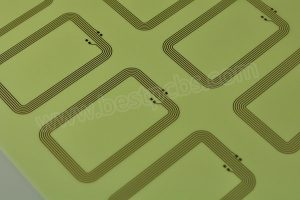
A homemade PCB is a printed circuit board created using DIY methods, often for prototyping or small-scale projects. Unlike professionally manufactured PCBs, which involve advanced processes and materials, homemade PCBs are made using simpler techniques such as etching, milling, or toner transfer. These methods are cost-effective and accessible for hobbyists and small-scale projects, though they may not match the precision and durability of professionally manufactured PCBs.
What Are the Advantages of Homemade PCB?
Advantages of homemade PCB:
- Cost-Effective: Affordable materials and tools for small-scale projects.
- Accessibility: Easy to create with basic equipment and materials.
- Customization: Flexibility to design and modify PCBs as needed.
- Learning Opportunity: Great for understanding PCB design and manufacturing processes.
- Additional Advantages of Homemade PCBs.
- Rapid Prototyping: Enables immediate design adjustments and functional testing, bypassing commercial fabrication delays.
- Enhanced Process Control: Direct oversight of etching, drilling, and soldering parameters ensures tailored quality for niche applications.
- Reduced Lead Times: Eliminates reliance on external vendors, accelerating project timelines for urgent iterations.
- Experimental Adaptability: Supports unconventional designs (e.g., mixed-signal layouts or hybrid materials) for research-specific needs.
- Skill-Driven Optimization: Enables manual refinement of trace geometries and impedance matching, critical for high-frequency circuits.
Applications of Homemade PCB Board
Applications of homemade PCB board:
- Prototyping: Testing and refining circuit designs before mass production.
- Hobby Projects: Creating small-scale electronics for personal use (e.g., LED controllers, audio amps).
- Education: Learning PCB design, soldering, and electronics fundamentals.
- Custom Electronics: Building unique or one-off devices (e.g., retro gaming consoles, smart home sensors).
- DIY Gadgets: Crafting specialized tools (e.g., 3D printer controllers, robotics modules).
- Repair and Modification: Fixing or upgrading existing circuits with tailored solutions.
- Art Installations: Designing interactive light displays or kinetic sculptures.
- IoT Devices: Developing low-cost connected sensors or smart home accessories.
- Robotics: Prototyping motor drivers, sensor interfaces, or control boards.
- Research and Development: Experimenting with novel circuit topologies or materials.
- Gift Making: Personalizing electronics (e.g., custom-engraved LED name tags).
- Environmental Monitoring: Building weather stations or pollution sensors for field use.
What are the Limitations of Homemade PCB board?
Limitations of homemade PCB board:
- Precision: Lower accuracy compared to professionally manufactured PCBs.
- Durability: Less robust and prone to wear and tear.
- Complexity: Limited to simpler designs and fewer layers.
- Time-Consuming: Requires more time and effort to produce.
- Material Limitations: Inability to utilize advanced substrates (e.g., high-frequency laminates) or precision finishes critical for specialized applications.
- Fault Detection Challenges: Lack of professional testing equipment complicates troubleshooting of hidden defects like micro-shorts.
- Scalability Issues: Manual processes hinder consistent reproduction for medium-to-large production batches.
How to Make a Homemade PCB?
Below are process of how to make a homemade PCB:
1. Design the PCB Layout
- Use EDA software (e.g., Autodesk Eagle, KiCad, or EasyEDA) to design your circuit schematic and PCB layout.
- Ensure proper component placement, signal routing, and adherence to design rules (e.g., trace width, spacing).
- Export the design as a Gerber file or printable format (e.g., PDF/PNG).
2. Prepare Materials and Tools
Materials:
- Copper-clad laminate (FR-4 recommended).
- Laser printer, glossy paper, or transparent film.
- Ferric chloride (FeCl₃) or ammonium persulfate (etching solution).
- Drill bit (0.5–1 mm for through-hole components).
- Sandpaper, gloves, and safety goggles.
Tools:
- Iron or laminator (for toner transfer).
- Drill press or hand drill.
- Plastic container for etching.
3. Print the PCB Layout
- Print the PCB layout as a mirror image on glossy paper using a laser printer.
- Ensure high contrast and no broken traces.
4. Prepare the Copper-Clad Board
- Cut the copper-clad board to size using a hacksaw or PCB cutter.
- Clean the copper surface with sandpaper to remove oxidation.
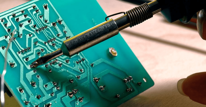
5. Transfer the Layout to the Board
- Toner Transfer Method:
- Place the printed glossy paper (ink-side down) on the copper board.
- Iron the paper at medium heat for 5–10 minutes.
- Soak the board in water to loosen the paper, then gently rub off the paper to reveal the toner pattern.
- Alternative: Use a UV exposure system with photoresist-coated boards for higher precision.
6. Etch the Board
- Submerge the board in ferric chloride solution (1 part FeCl₃ to 2 parts water).
- Agitate gently for 15–30 minutes until excess copper is dissolved.
- Rinse thoroughly with water and remove the toner with acetone.
7. Drill Holes
- Use a drill press or hand drill to create holes for components.
- Reference the Gerber file for precise hole locations.
8. Apply Solder Mask and Silkscreen (Optional)
- Paint the board with liquid solder mask or use a UV-curable mask for protection.
- Add component labels using a silkscreen pen or laser printer toner transfer.
9. Finish and Test
- Clean the board with isopropyl alcohol.
- Apply a thin layer of solder flux and tin the traces if needed.
- Assemble components and test for continuity/shorts using a multimeter.
10. Safety Precautions
- Wear gloves and work in a well-ventilated area when handling chemicals.
- Dispose of etching solution responsibly (check local regulations).

Why Choose Professional PCB Manufacturing?
While homemade PCBs are great for small projects, professional PCB manufacturing offers:
- High Precision: Advanced processes for accurate and reliable PCBs.
- Durability: Robust materials and finishes for long-lasting performance.
- Complex Designs: Support for multi-layer and high-density designs.
- Scalability: Efficient production for large-scale projects.
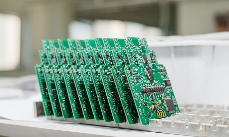
Our Professional PCB Services
At EBest Circuit (Best Technology), we offer comprehensive PCB manufacturing services, including:
- Custom Design: Tailored solutions to meet your specific requirements.
- Material Selection: High-quality materials for optimal performance.
- Precision Manufacturing: Advanced processes for accurate and reliable production.
- Quality Assurance: Rigorous testing to ensure reliability and performance.
Why Choose Us for Your PCB Needs?
EBest Circuit (Best Technology) stands out as a trusted partner for homemade PCB manufacturing, offering tailored solutions to meet your unique needs. Here’s why we are the ideal choice:
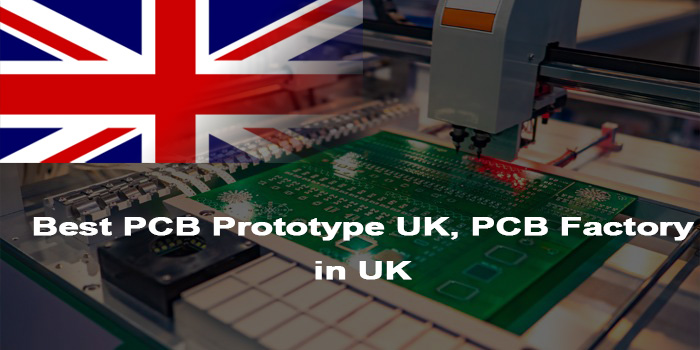
Lightning-Fast Lead Times & 24-Hour Rapid Prototyping
- 24-hour sample delivery: Receive your PCB prototypes within 24 hours of approval, accelerating your product development cycle.
- Urgent order support: Expedited production for time-sensitive projects, ensuring you never miss a deadline.
Customized Sample Production with No MOQ
- Minimum order quantity (MOQ) = 1 piece: Perfect for prototypes, small-batch hobby projects, or niche custom designs.
- Flexible customization: Tailor specifications (e.g., layer count, trace width, materials) to match your exact requirements.
Free DFM Analysis to Optimize Costs
- Design for Manufacturability (DFM) checks: Our engineers analyze your design for potential issues (e.g., trace spacing, via placement) at no cost, preventing costly revisions later.
- Cost-saving recommendations: Identify opportunities to reduce material waste and streamline production without compromising quality.
Pre-Sales & After-Sales Support
- Multilingual team: Instant assistance via chat, email, or phone in English, Chinese, and other languages.
- Technical expertise: Engineers provide real-time guidance on design, material selection, and troubleshooting.
Guaranteed Post-Sales Support
- Quality assurance: Rigorous testing (e.g., electrical tests, AOI inspections) ensures defect-free boards.
- Hassle-free returns/replacements: Quick resolution for any issues, backed by our commitment to customer satisfaction.
- Long-term partnership: Ongoing support for revisions, scaling, or future projects.
Contact Us Today
Whether you need homemade PCBs for prototyping or professional PCBs for large-scale production, EBest Circuit (Best Technology) is here to help. Contact us today to discuss your PCB needs and get a quote: sales@bestpcbs.com.
You may also like


Tags: Homemade PCB, Homemade PCB Board