Discover everything about 2-layer PCB, including their advantages, applications, manufacturing process, and why EBest Circuit (Best Technology) is the ideal partner for your PCB needs.
What is a 2-Layer PCB?
A 2-Layer PCB, also known as a double-layer PCB, is a printed circuit board that consists of two conductive copper layers. These layers are located on the top and bottom surfaces of the board, separated by an insulating substrate material. 2-Layer PCBs are widely used in electronic devices due to their ability to support more complex circuits than single-layer PCBs while remaining cost-effective and relatively simple to manufacture.
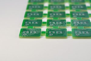
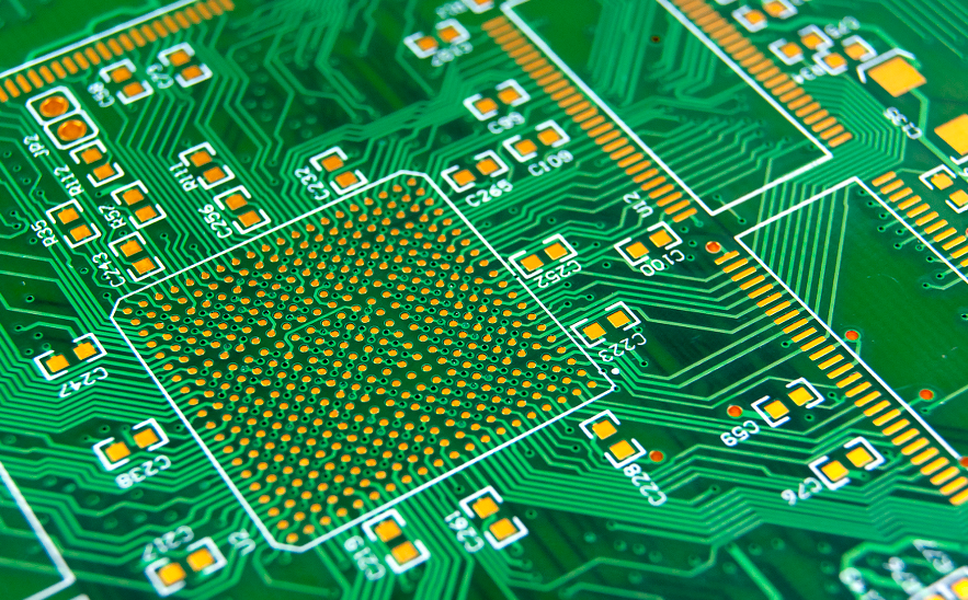
2-Layer PCB
What are the Advantages of 2-Layer PCB?
- Increased Circuit Complexity: Allows for more intricate designs by utilizing both sides of the board.
- Cost-Effective: Balances functionality and affordability, making it ideal for many applications.
- Compact Design: Enables space-efficient layouts, perfect for devices with limited space.
- Improved Signal Integrity: Reduces electromagnetic interference (EMI) and enhances performance.
- Versatility: Suitable for a wide range of industries, from consumer electronics to industrial equipment.
What are the Advantages of 2-Layer PCBs?
What Problems Can 2-Layer PCBs Solve?
2-Layer PCB address several challenges in electronic design and manufacturing:
- Space Constraints: Compact designs for devices with limited space.
- Circuit Complexity: Supports more complex circuits without the cost of multi-layer PCBs.
- Signal Interference: Minimizes EMI and crosstalk for better performance.
Applications of 2-Layer PCBs
2-Layer PCB are used in various industries and applications, including:
- Consumer Electronics: Smartphones, tablets, and home appliances.
- Industrial Equipment: Control systems and automation devices.
- Automotive Electronics: Sensors, control units, and infotainment systems.
- Medical Devices: Diagnostic equipment and monitoring systems.
- Telecommunications: Routers, modems, and communication devices.
Our Services for 2-Layer PCBs
At EBest Circuit (Best Technology), we offer comprehensive services for 2-Layer PCB, including:
- 2-Layer PCB Design: Customized design solutions tailored to your needs.
- 2-Layer PCB Prototyping: Fast and accurate prototyping to validate your design.
- 2-Layer PCB Manufacturing: High-quality production adhering to industry standards.
- 2-Layer PCB Assembly: Full assembly services, including SMT and thru-hole components.
Why Choose Us for 2-Layer PCBs?
- 18+ Years of Experience: Proven expertise in delivering high-quality PCBs.
- Competitive Pricing: Affordable solutions without compromising quality.
- Quick Turnaround: Expedited services with 24-hour shipping for urgent orders.
- ISO-Certified Quality: Adherence to IPC standards, including Class 2, Class 3, and Class 3A.
2-Layer PCB Manufacturing Capabilities
| Parameter | Capability |
|---|---|
| Layers | 2 |
| Material | FR4, Aluminum, Ceramic, etc. |
| Board Thickness | 0.4mm – 3.2mm |
| Copper Thickness | 0.5oz – 6oz |
| Minimum Trace/Space | 3mil/3mil |
| Surface Finish | HASL, ENIG, OSP, etc. |
| Solder Mask | Green, Blue, Red, etc. |
| Silkscreen | White, Black, etc. |
How is a 2-Layer PCB Different from Other PCBs?
- Single-Layer PCBs: Only one conductive layer, limiting circuit complexity.
- Multi-Layer PCBs: Three or more layers, offering higher complexity but at a higher cost.
- 2-Layer PCBs: Two conductive layers, balancing complexity and cost-effectiveness.
If you have any questions about 2-Layer PCBs or would like to request a quote, feel free to contact us. We are committed to providing the best quality, pricing, and services to meet your PCB needs.