





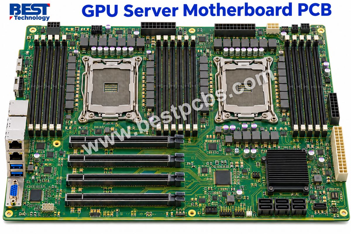
A GPU server motherboard PCB provides the electrical connections for CPUs, memory, storage and GPU interfaces inside a server. Some systems connect GPU cards through PCIe slots or risers, while others use a separate GPU baseboard. This difference affects the motherboard’s layout, layer count and manufacturing requirements.
For a custom server project, the GPU connection method helps define the board before material or layer selection begins. Direct PCIe connections need enough CPU lanes and routing space, while a separate GPU baseboard moves part of the GPU interconnection away from the host motherboard.
At EBest Circuit (Best Technology), we provide multilayer PCB fabrication, component sourcing and assembly for custom electronic hardware. Our engineering team reviews the board construction and assembly files so customers can move from a motherboard design to prototype and production builds.
Key Takeaways
- The host motherboard connects CPUs, system memory and server interfaces, while a separate GPU baseboard carries GPU modules and their platform-specific connections.
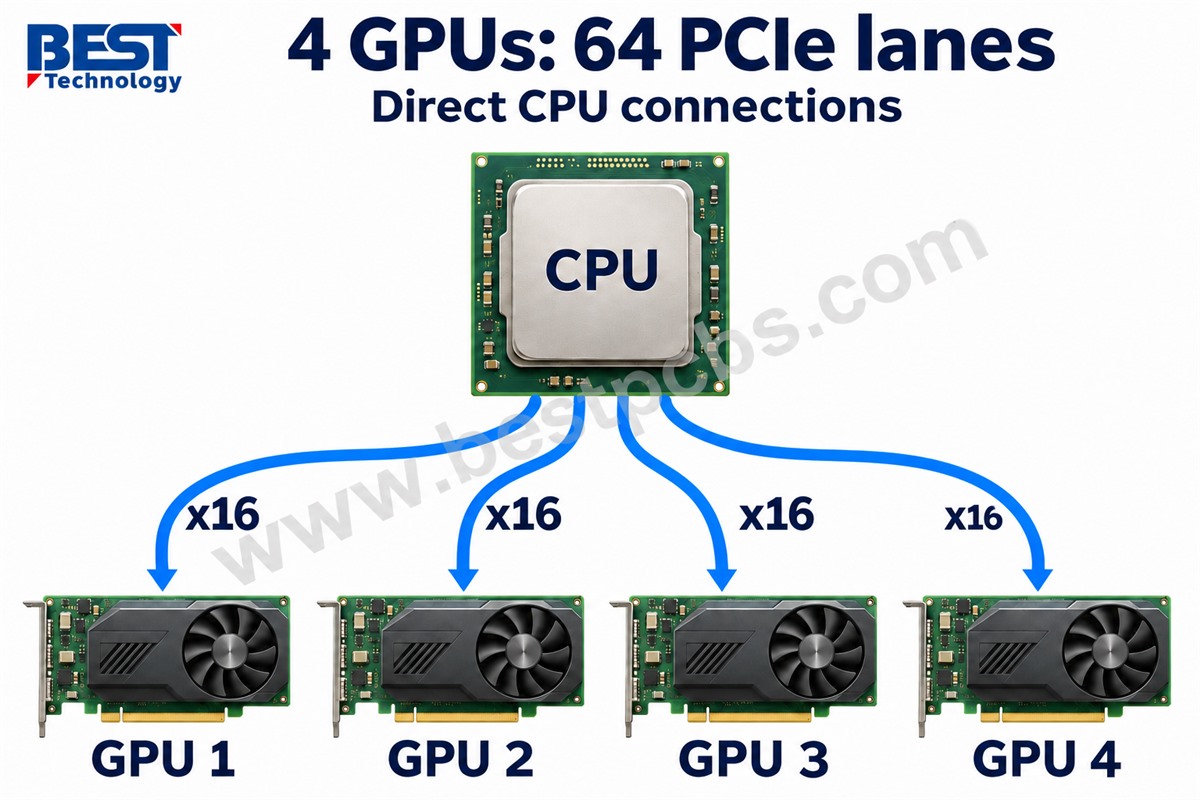
- 4 GPUs connected directly at x16 require 64 CPU PCIe lanes before storage, networking and other PCIe devices are counted.
- Motherboard layer count follows routing density, reference planes and power distribution rather than GPU quantity alone.
- Low-loss laminates help long or demanding PCIe channels, while a high Tg value describes thermal behavior rather than electrical loss.
- HDI and via-in-pad help dense component routing, whereas backdrilling removes unused via sections that can disturb high-speed signals.
- Bare-board electrical tests, assembly inspection and powered functional tests check different stages of motherboard production.
What Is a GPU Server Motherboard PCB?
A GPU server motherboard PCB is the multilayer circuit board that supports the host processor, memory and interfaces used by a GPU-equipped server. Copper traces carry signals between devices, power and ground layers distribute current, and insulating layers separate the copper circuitry.
The bare PCB becomes an assembled motherboard after sockets, connectors, voltage regulators and other components are installed. Its layout may include direct GPU slots, connectors for risers or cables leading to a separate accelerator assembly. The motherboard therefore does not need to carry the GPU chips themselves.
Common applications include:
- AI training servers that move data between host processors, storage and multiple accelerators.
- Inference servers that combine GPU processing with network and storage interfaces.
- High-performance computing systems used for simulation, scientific calculations and parallel workloads.
- Rendering servers that support multiple GPU cards within a rack-mounted system.
The broader AI server PCB category also includes accelerator boards, network boards and power distribution boards, each with a different manufacturing role.
GPU Server Motherboard vs GPU Baseboard: What Is the Difference?
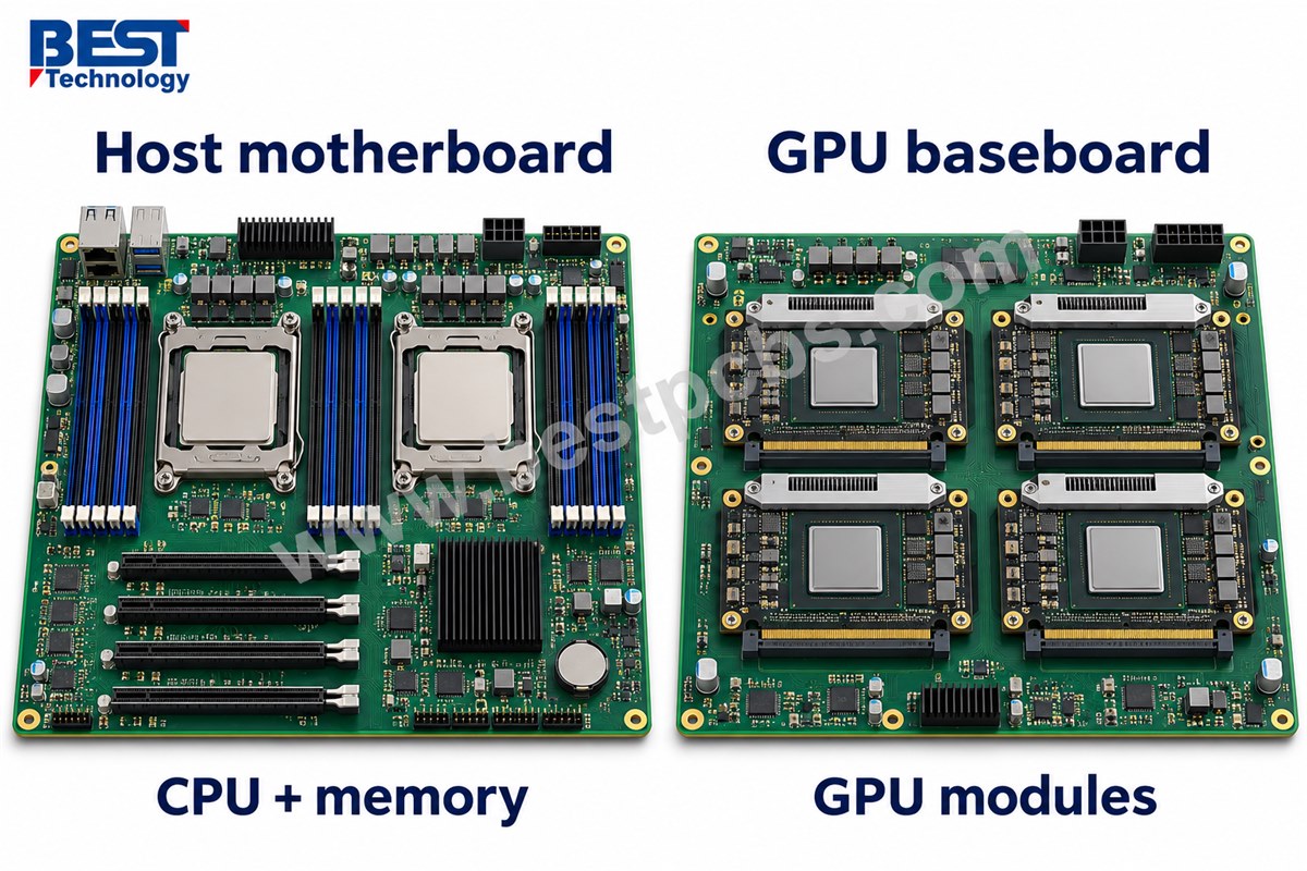
The host motherboard manages the CPU, system memory and server I/O, while a GPU baseboard connects accelerator modules and the interfaces required by that GPU platform. PCIe GPU cards are another board type, with the GPU and its local circuitry mounted on each card.
| Board type | Main components | Main connection role |
|---|---|---|
| Host motherboard | CPU sockets, DIMM sockets, management circuitry and system connectors | Connects host processing, memory, storage, networking and GPU interfaces |
| GPU baseboard | GPU module connectors, power circuitry and, on some platforms, dedicated interconnect switches | Connects accelerator modules to each other and to the host system |
| PCIe GPU card | GPU, local memory, voltage regulators and PCIe interface | Adds an accelerator through a PCIe slot or riser |
This distinction matters when discussing a manufacturing project. A request for an 8 GPU server motherboard may refer to a host board serving a separate accelerator assembly rather than a PCB with 8 GPUs mounted directly on it. The system block diagram identifies which board the customer actually needs fabricated.
How Does a Server Motherboard Connect Multiple GPUs?
Server motherboards connect multiple GPUs through CPU PCIe links, either directly or through risers, PCIe switches and platform-specific baseboard connections. The number of usable GPUs depends on the available lanes, connection topology and system support.
For a multi GPU server motherboard, the main connection options are:
- Direct CPU connections give each GPU a dedicated PCIe link, with the CPU lane count setting the available link widths.
- Risers relocate GPU cards to fit the chassis and may carry 1 or several links, depending on their design.
- PCIe switches connect multiple downstream devices through upstream CPU links, with upstream bandwidth shared when traffic exceeds that connection’s capacity.
- Separate GPU baseboards provide the module connections and interconnect arrangement required by the selected accelerator platform.
For full-width direct connections, the lane requirement is:
GPU PCIe lanes = number of GPUs × lanes per GPU
A 4 GPU configuration using x16 for every card therefore requires 4 × 16 = 64 lanes. NVMe drives and network adapters need their own allocation. A switch-based design may use fewer upstream CPU lanes, but it changes how the GPUs share bandwidth.
Slot length alone does not establish lane width. A physical x16 connector can be wired for x8, so the motherboard’s electrical configuration matters more than the appearance of the slot.
How Many PCB Layers Does a GPU Server Motherboard Need?
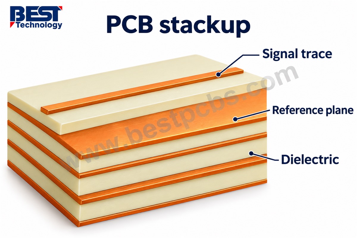
The required layer count comes from CPU, memory and PCIe routing, together with the reference planes and copper needed for power distribution. GPU count alone cannot determine that number.
The main demands on the stackup are:
- CPU sockets and memory channels consume routing space around dense pin fields.
- PCIe links need room for differential pairs and separation from neighboring signals.
- Ground planes provide nearby return paths for high-speed signals.
- Power layers distribute several voltage rails without forcing current through narrow copper sections.
- Board thickness must remain compatible with connectors, sockets and plated-hole manufacturing.
For example, adding signal layers to a proposed 20 layer board may relieve routing congestion, but those layers also need appropriate reference planes and dielectric spacing. Moving to 22 layers only helps when the revised stackup solves a specific routing or power requirement.
The stackup should show each layer’s function, copper thickness and finished dielectric thickness. Our AI server PCB design guide explains how those choices connect to signal integrity and power delivery.
Which PCB Materials Suit GPU Server Motherboards?
High Tg FR-4 can suit less demanding channels, while low-loss laminates are better candidates when long routes, faster interfaces or multiple connectors consume more of the signal-loss budget. The choice comes from the complete channel, not simply the word “server.”
The material properties answer different questions:
- Df, or dissipation factor, describes dielectric loss and helps assess signal attenuation.
- Dk, or dielectric constant, affects impedance and propagation delay.
- Tg, or glass transition temperature, describes a change in the resin’s mechanical behavior as temperature rises.
- Copper roughness affects conductor loss, particularly at higher frequencies.
High Tg and low loss are separate properties. A thermally robust FR-4 grade can still have too much electrical loss for a demanding channel.
The following MEGTRON 6 examples show why the exact laminate construction matters even within the same material family:
| Material grade | Glass type | Typical Dk at 13 GHz | Typical Df at 13 GHz | Tg by DSC |
|---|---|---|---|---|
| R-5775(N) | Low-Dk glass | 3.34 | 0.0037 | 185°C |
| R-5775(K) / R-5775(G) | Normal glass | 3.62 | 0.0046 | 185°C |
These typical values use a 0.75 mm test sample, with Dk and Df measured by the balanced-type circular disk resonator method. Impedance calculations also need the dielectric thickness and copper construction used for the actual board.
For material selection, our high-speed PCB materials guide explains the differences between FR-4 and low-loss options. Hybrid stackups can combine compatible material systems, but their lamination behavior and thermal expansion need to work together.
How Does PCIe Generation Affect PCB Routing?
Higher PCIe generations leave less room for signal loss and distortion, making trace length, copper roughness, connectors and via transitions more demanding parts of the PCB design.
| PCIe generation | Transfer rate per lane | Signaling |
|---|---|---|
| PCIe 4.0 | 16 GT/s | NRZ |
| PCIe 5.0 | 32 GT/s | NRZ |
| PCIe 6.0 | 64 GT/s | PAM4 |
GT/s describes the interface transfer rate; usable application throughput also depends on encoding and protocol overhead. PCIe 6.0 uses 4 signal levels rather than the 2 levels used by NRZ, changing the signal-quality requirements.
Signals lose strength as they travel through motherboard traces, connectors, risers and the GPU card. The design must account for that complete path, so shortening a route or removing an unnecessary layer transition can be as useful as changing the laminate.
Practical routing priorities include continuous reference planes, differential-pair geometry matched to the platform impedance target, and controlled spacing from adjacent signals. Retimers can restore signal timing on channels that need them, but they add components, power and placement requirements.
How Does the Motherboard Supply Power to CPUs, Memory and GPU Slots?
The motherboard receives power through its input connectors and distributes it through copper planes, vias and voltage regulator circuits to the CPU, memory and expansion interfaces. GPU cards or baseboards may also use separate power connections for their larger loads.
Voltage regulator modules, or VRMs, convert an input supply into the lower voltages required by processors and other devices. Low voltage can still mean high current: an illustrative 200 W load at 1.0 V requires 200 A at the load, using I = P / V.
That current makes copper resistance significant. For example, 100 A through a 0.5 mΩ path produces a 0.05 V drop and 5 W of heat, from V = I × R and P = I² × R. Here, R represents the total resistance of the path being evaluated, including its relevant copper and connections.
The layout therefore needs enough copper cross-section, suitable via connections and short paths between regulators and loads. Narrow necks around pads, cutouts or mounting holes can become restrictions even when the rest of the power plane is large.
The motherboard power budget should include the loads it actually supplies. GPU auxiliary cables and separate baseboard inputs may carry much of the accelerator power through a different route.
When Are HDI, Via-in-Pad and Backdrilling Needed?
HDI and via-in-pad help route dense component connections, while backdrilling reduces the electrical effect of unused plated-hole sections. Each process solves a different PCB problem.
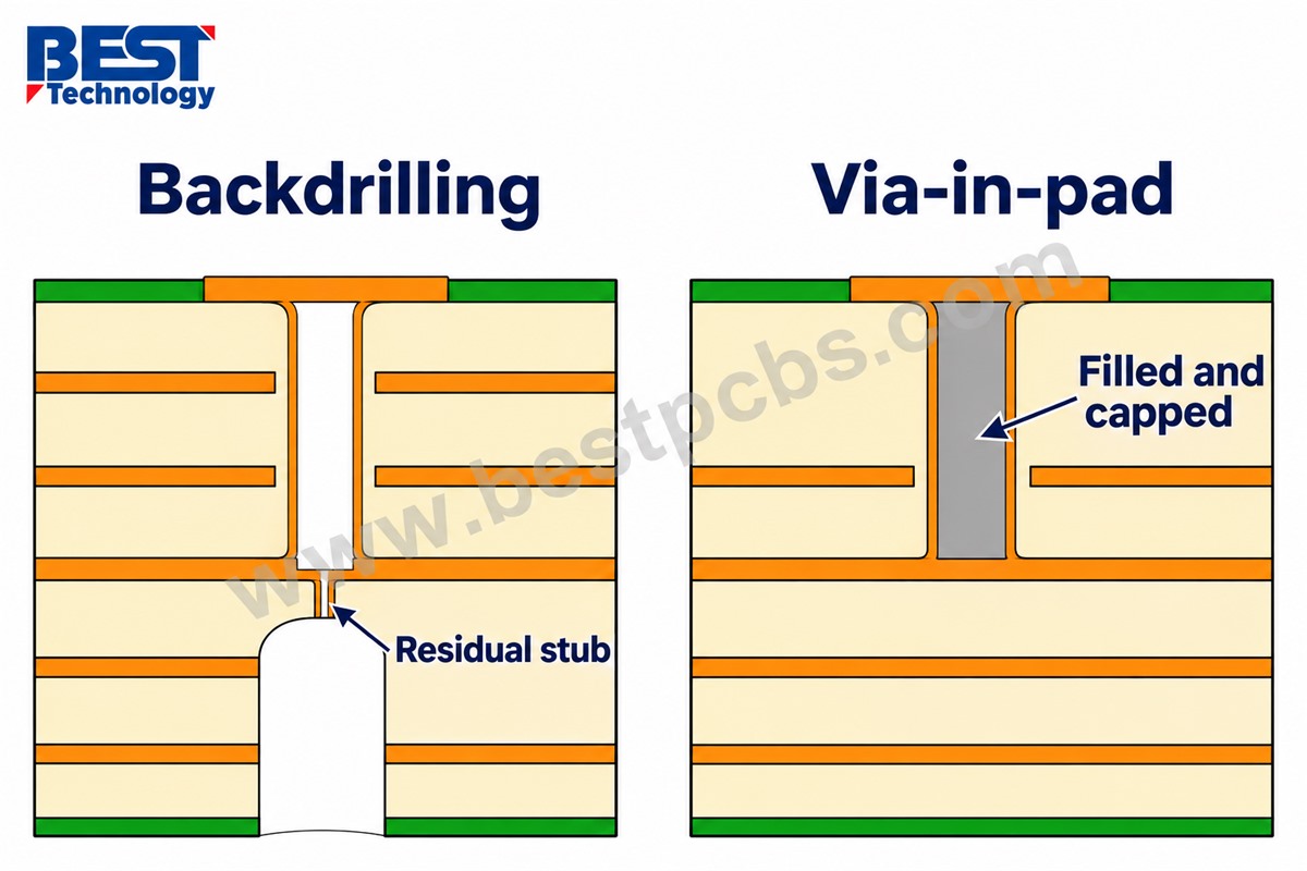
- HDI uses small vias and additional interconnect structures to route dense pin fields where conventional through-holes take too much space.
- Via-in-pad places a connection inside a component pad, allowing a shorter route to another layer; solderable pads commonly require filled and capped structures to prevent solder from draining into the hole.
- Backdrilling removes the unused portion of a plated through-hole after plating, reducing the residual via stub on a high-speed signal path.
For example, a through-hole via connecting an outer layer to a nearby inner layer can leave a long unused barrel extending through the rest of a thick board. Backdrilling removes most of that unused section while preserving the intended connection.
Fine-pitch component routing may justify HDI even on a relatively short signal path. Conversely, a thick board can need backdrilling on selected PCIe vias without requiring microvias throughout the design. The pad layout and channel requirements identify where each process adds value.
How Do Cooling and Board Size Affect Motherboard Layout?
Cooling hardware and chassis dimensions determine where sockets, memory, connectors and mounting points can fit on the motherboard. These mechanical requirements need space in the layout before routing begins.
The main layout considerations are:
- CPU heat sinks need mounting space and clearance from DIMM sockets, power components and cables.
- Air-cooled systems need airflow through the component area rather than tall connectors blocking the intended path.
- Liquid-cooled systems need clearance for cold plates, fittings and hoses, including access during assembly.
- GPU risers and cables must align with their chassis positions without straining motherboard connectors.
- Large boards need suitable support around heavy heat sinks and connector insertion points.
Board outline, component height limits and mounting-hole positions belong in the mechanical design supplied to the PCB and assembly teams. Changing them after routing can move connectors or interrupt copper areas that the electrical design already uses.
What Does GPU Server Motherboard PCB Assembly and Testing Require?
GPU server motherboard assembly requires controlled solder-paste deposition, accurate component placement and a reflow process suited to large sockets, connectors and areas with different copper mass. Inspection and electrical testing then check the board at successive production stages.
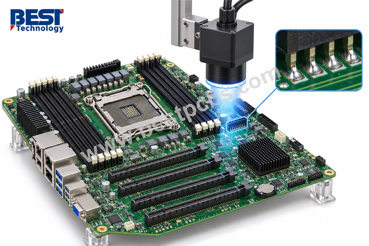
Large connectors and power components absorb heat differently from small surface-mount devices. The assembly process needs to form their joints without overheating more sensitive components. Board supports can help maintain flatness during printing, placement and soldering, especially on large assemblies.
| Production stage | Main checks |
|---|---|
| Bare PCB | Continuity and isolation, dimensions, plated-hole quality and specified impedance coupons |
| Solder-paste printing | Paste volume, alignment and deposits that could cause bridges or insufficient joints |
| After component assembly | Component position, polarity, visible joints and hidden solder connections where X-ray inspection applies |
| Powered functional testing | Voltage rails, startup, memory detection and agreed communication or interface functions |
TDR checks impedance behavior on the measured structure. PCIe link qualification additionally requires the platform’s applicable electrical and system tests; passing a coupon measurement alone does not establish link compliance.
For functional testing, the build plan identifies the required CPUs, memory, firmware, fixtures and test procedure. This allows the assembly supplier to quote and perform a defined test rather than treating “fully tested” as an unspecified promise.
Why Choose EBest Circuit for GPU Server Motherboard PCB Manufacturing?
EBest Circuit brings PCB fabrication, component sourcing and assembly into the same manufacturing project, helping customers coordinate the bare-board construction with the parts and processes needed for the finished motherboard.
Our FR-4 PCB manufacturing capabilities include the following process options:
| Manufacturing item | Capability |
|---|---|
| Layer count | 1–10 layers in the standard process; special-process builds up to 32 layers |
| Material requirement | High Tg material for 8 layers and above |
| Laser via diameter | 0.10 mm |
| Inner-layer trace/space with 1 oz copper | 4/4 mil standard; 3/3 mil with special processing |
| Through-hole aspect ratio | 8:1 standard; 10:1 with special processing |
Our engineers assess the selected layer count, hole structure and copper geometry together before confirming a special-process motherboard build.
Our PCB assembly services combine manufacturing equipment with support for the customer’s component and test requirements:
- Yamaha YSM20R placement equipment supports surface-mount assembly, with 3D SPI checking solder-paste deposits before component placement.
- Nitrogen reflow and through-hole assembly processes support boards containing a mixture of small devices, sockets and larger connectors.
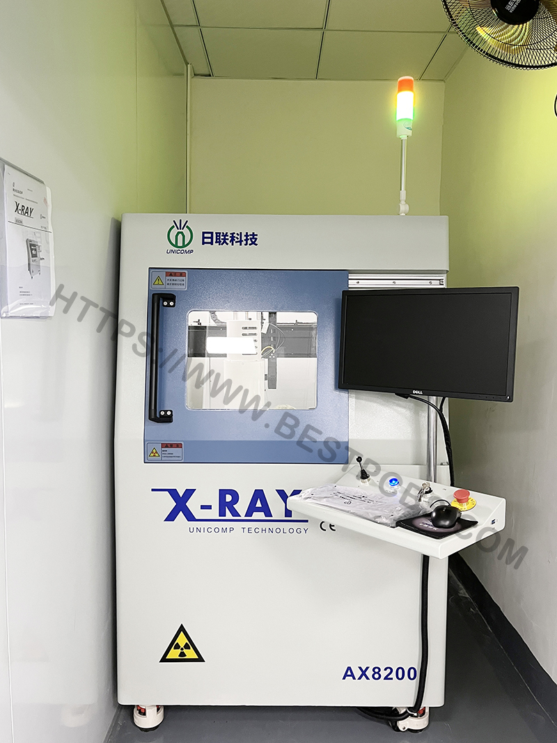
- AOI and X-ray inspection help examine component placement and solder connections, including joints hidden beneath suitable component packages.
- Customers can use our component sourcing service or provide selected parts, with BOM and incoming-material checks before assembly.
- Functional testing can follow an agreed procedure using the firmware, hardware and fixtures required by the project.
For prototype and production orders, we review the fabrication files, BOM and assembly requirements together so material availability, component packages and manufacturing details can be resolved before the build.
FAQ
Can an x16 PCIe slot operate with only 8 lanes?
Yes. A physical x16 slot can be wired for x8 operation, and a compatible device can use that narrower connection. At the same PCIe generation, x8 provides half the lane bandwidth of x16, although the effect on the workload depends on how much data it transfers through PCIe.
Does a PCIe retimer add more PCIe lanes?
No. A retimer restores signal timing and quality along an existing link; it does not create additional CPU lanes or act as a multi-device PCIe switch. Its role is to help a channel meet signal requirements across the planned connection.
Does a custom motherboard PCB order include BIOS or BMC firmware?
Not automatically. Bare-board fabrication supplies the PCB, while assembly installs the specified components. BIOS and baseboard management controller firmware, programming and startup testing need a defined project scope, including the required software files and any licensing arrangements.
Can EBest Circuit assemble a motherboard using customer-supplied components?
Yes. Customers can provide selected components while we source the remaining BOM items. The assembly plan identifies which parts come from each source, their package and quantity, and any handling requirements before production begins.
Can prototype and production builds use the same approved stackup?
Yes, provided the materials and construction remain available and suitable for the production process. Using the intended production stackup for prototypes reduces changes between electrical validation and volume manufacture; a material or dielectric-thickness change can require renewed impedance and channel checks.
Conclusion
GPU server motherboard PCB design starts with the host architecture and GPU connections, then develops into a stackup, material choice and manufacturing process that support those requirements. Clear separation between the motherboard, accelerator boards and power paths helps customers choose the right construction without adding unnecessary complexity.
For a custom motherboard PCB or assembly project, send your fabrication files, stackup requirements, BOM and target quantity to sales@bestpcbs.com. EBest Circuit can review the manufacturing scope and discuss prototype or production options with your team.
You may also like




Tags: 8 gpu server motherboard, gpu server motherboard, GPU Server Motherboard PCB, gpu server motherboards, multi gpu server motherboard