





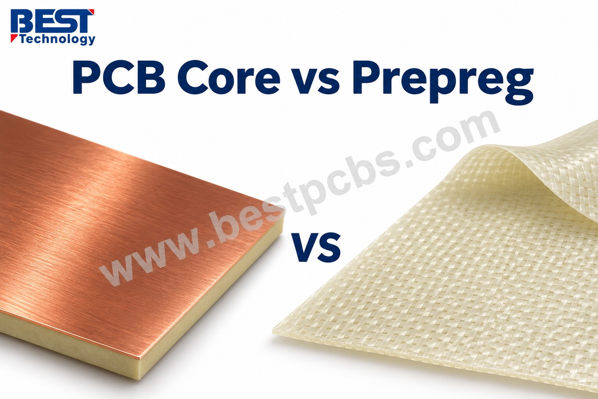
The main difference in PCB core vs prepreg is their condition before lamination: core is a cured laminate that supports copper circuitry, while prepreg contains partially cured resin that bonds the layers together. Both provide electrical insulation in a multilayer PCB, but they perform different jobs during manufacturing.
For a multilayer control board, communication module, or industrial controller, the combination determines how the copper layers fit within the required board thickness. It also sets the spacing between signal traces and reference planes, which affects controlled impedance.
At EBest Circuit (Best Technology), we manufacture FR-4 PCBs, including multilayer boards, high glass transition temperature (high-Tg) materials, and high-density interconnect (HDI) constructions. We support prototype fabrication, volume production, and assembly, with core and prepreg combinations selected around the board’s routing, thickness, and electrical requirements.
Key Takeaways
- Core supports etched copper circuits, while prepreg flows around the copper and bonds adjacent layers during lamination.
- A common 4-layer foil-built PCB uses 1 copper-clad core for L2 and L3, with prepreg bonding the outer copper foils to the core.
- The prepreg dimension used for impedance design is the finished dielectric spacing, which changes with resin content, copper coverage, and lamination conditions.
- 1080, 2116, and 7628 identify glass fabric styles, so the resin system and resin content are also needed to define thickness and Dk.
- Increasing trace-to-plane spacing generally raises impedance, while increasing Dk generally lowers it when the other design variables remain unchanged.
- Prepreg cannot directly replace a copper-clad core, because the replacement must also preserve the circuit layers and their manufacturing sequence.
- Stocked core thicknesses and prepreg constructions can reduce sourcing costs, while special material grades and additional lamination cycles add expense.
What Is a PCB Core?
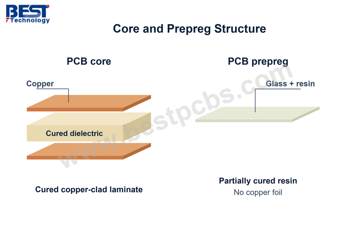
A PCB core is a cured insulating laminate, commonly supplied with copper foil bonded to 1 or both sides. In a conventional FR-4 board, woven glass reinforces an epoxy resin system. The cured material holds its shape while the fabricator forms circuits on the copper.
For a multilayer PCB, the fabricator images and etches the core’s copper before placing it into the final stack. These circuits become internal signal layers, power planes, or ground planes after lamination. The dielectric between the 2 copper faces keeps them electrically separated.
Common uses include:
- 2-layer boards: A copper-clad core provides the substrate for the top and bottom circuits.
- Multilayer inner layers: Patterned cores carry circuits that will sit inside the finished board.
- Defined dielectric spacing: The cured laminate establishes the separation between its 2 copper faces.
Despite its name, a core does not have to occupy the center of the board. Multilayer constructions can contain several cores at different positions in the stack.
What Is PCB Prepreg?
PCB prepreg is woven glass fabric impregnated with partially cured resin. In conventional FR-4 prepreg, the epoxy resin is in the B-stage: it is partly cured but can still soften and flow when heated during lamination.
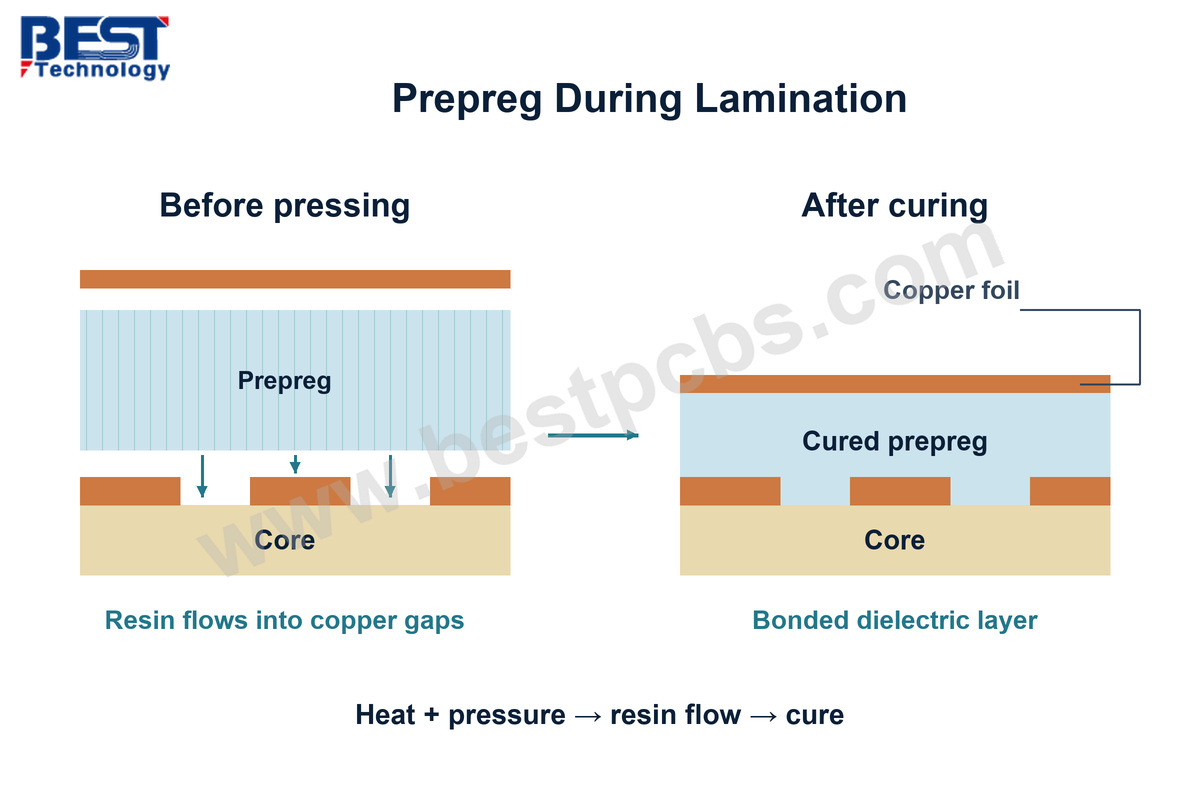
Fabricators place prepreg between inner-layer cores and beneath the outer copper foils. Heat and pressure make the resin flow into the gaps around etched copper and bond the layers together. As the resin cures, it forms a solid insulating layer that keeps neighboring copper layers electrically separated.
Unlike a copper-clad core, prepreg is supplied without copper foil. The circuit comes from copper on the core or from separately added foil; prepreg provides the bond and insulation between those copper layers.
PCB Core vs Prepreg: Key Differences
Core holds the copper circuits on a cured laminate, while prepreg bonds the circuit layers together during pressing. Most conventional multilayer designs need both.
| Comparison | PCB core | PCB prepreg |
|---|---|---|
| Resin condition before lamination | Cured laminate | Partially cured, B-stage resin |
| Copper as supplied | Commonly copper-clad on 1 or both sides | Normally supplied without copper foil |
| Circuit formation before final pressing | Copper can be imaged and etched | No copper foil to etch before lamination |
| Behavior during lamination | Retains its established laminate structure | Resin flows, bonds surfaces, and completes curing |
| Main role | Supports circuits and provides insulation | Bonds layers and provides insulation |
| Thickness basis | Existing cured laminate thickness | Finished dielectric thickness after pressing |
| Typical position | Substrate of a 2-layer board or internal laminate in a multilayer board | Between cores or beneath outer copper foil |
How Are Core and Prepreg Used in a PCB Stackup?
Core carries the inner-layer circuits, while prepreg bonds the cores and outer copper foils into a multilayer board. The layer count determines how many circuit layers the construction must accommodate.
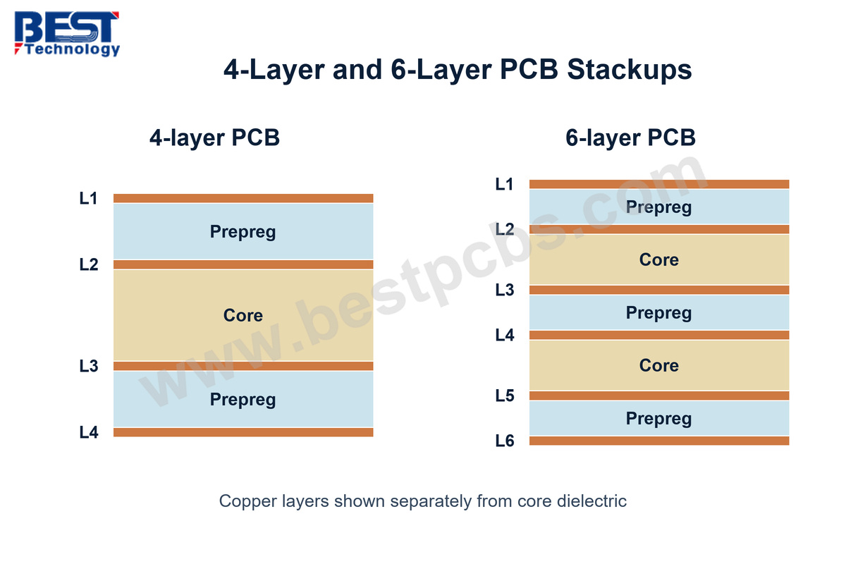
- 4-layer foil-built PCB: 1 copper-clad core carries L2 and L3, with prepreg on both sides bonding the separate copper foils for L1 and L4.
- 6-layer foil-built PCB: 2 copper-clad cores carry L2–L3 and L4–L5, with prepreg between the cores and beneath the outer foils for L1 and L6.
The fabricator etches the inner-layer circuits before lamination and forms the outer-layer circuits afterward. Each prepreg section may contain 1 or several plies to provide the required dielectric spacing and enough resin to fill the copper pattern.
These are common foil-built arrangements, not the only possible stackups. Blind vias, buried vias, and sequential lamination can require a different layer construction or pressing sequence.
Can You Replace a PCB Core Layer with Prepreg?
No, prepreg is not a direct replacement for a copper-clad core. Matching the nominal thickness does not preserve the core’s copper layers or its role in the manufacturing sequence.
For example, the core in the 4-layer construction above carries L2 and L3 before final lamination. Replacing it with a loose prepreg sheet would remove the substrate supporting those patterned layers. Keeping the same circuits would require a different copper arrangement and manufacturing process.
A redesigned stackup can use a different balance of cores and prepreg, but that change may affect:
- Copper-layer construction: Which circuits are patterned before each lamination step.
- Via formation: When the fabricator drills and plates buried or blind connections.
- Electrical spacing: The distance between signals and their reference planes.
- Pressing sequence: The number of lamination steps and the materials bonded during each step.
PCB Core vs Prepreg Thickness: What Is the Difference?
PCB core and prepreg thickness differ in how they are specified: core has an already-cured thickness, while prepreg must achieve the required thickness during pressing. For electrical design, the useful dimension is the finished dielectric spacing between copper layers.
Core specifications may state dielectric-only thickness or total copper-clad thickness. Those values differ because copper contributes to the total. For example, a 0.200 mm dielectric with 0.035 mm copper on each face has a nominal copper-clad thickness of 0.270 mm.
Prepreg requires a different calculation because some resin fills the spaces beside etched traces. Glass style, resin content, remaining copper area, and press conditions determine how much dielectric remains between adjacent copper surfaces. The thickness of an unpressed sheet is therefore not a reliable substitute for the finished spacing.
For a simple stackup thickness calculation:
T = Σt(core dielectric) + Σt(pressed prepreg dielectric) + Σt(copper)
Here, T is the laminate-and-copper thickness, and each t is a layer thickness in millimeters. Solder mask and surface finish are outside this simplified calculation.
For an illustrative 4-layer stack with a 1.000 mm core dielectric, 2 0.200 mm finished prepreg sections, and 4 0.035 mm copper layers:
T = 1.000 + (2 × 0.200) + (4 × 0.035) = 1.540 mm
The calculation includes each copper layer without duplication. If the starting core dimension already includes its copper, adding that copper again would overstate the total. In a production stackup, finished outer copper also includes the applicable plating buildup.
The 1.540 mm result is a nominal sum, not a guaranteed finished-board measurement. Material tolerances, resin flow, and finished copper thickness can shift the actual result, so a board-thickness requirement needs an acceptance tolerance as well as a nominal value.
For a 1.60 mm, 4-layer board with 50 Ω outer-layer traces, material selection works in the opposite direction:
- The signal-to-plane spacing comes first: If the impedance design calls for 0.200 mm between L1–L2 and L3–L4, those gaps set the 2 finished prepreg sections.
- The remaining thickness sets the core target: With 0.035 mm finished copper on each of the 4 layers, the simplified dielectric budget is 1.600 − (2 × 0.200) − (4 × 0.035) = 1.060 mm for the core dielectric.
- Available materials determine the production combination: If a 1.060 mm core is unavailable, the fabricator can propose a nearby core and adjust the prepreg construction, then recalculate the trace width for the revised spacing.
This example reserves the outer dielectric gaps for impedance control instead of dividing the board thickness equally among all insulating layers. The 1.060 mm value is a calculated target, not a claim that this core thickness is stocked; the final stackup must also meet the drawing’s thickness tolerance and measurement requirements.
Core is not automatically thicker than prepreg. Thin cores and multiple prepreg plies can reverse that relationship.
What Do 1080, 2116 and 7628 Mean in a PCB Stackup?
1080, 2116, and 7628 are woven glass fabric style designations. They describe the reinforcement construction, rather than a complete PCB material grade or a fixed finished thickness.
For conventional glass-epoxy materials, 1080 generally supports thinner dielectric constructions, 2116 occupies an intermediate range, and 7628 uses a heavier fabric suited to thicker constructions. The resin content changes the finished properties within each style.
The following Isola 370HR prepreg examples, from Dk/Df Tables Revision I, February 24, 2026, show how glass style and resin content affect listed thickness and dielectric constant (Dk) at 1 GHz. These construction-specific values are not guaranteed pressed spacings for every copper pattern.
| Glass style | Resin content | Listed thickness, mm | Listed thickness, mil | Dk at 1 GHz |
|---|---|---|---|---|
| 1080 | 66% | 0.076 | 3.0 | 3.90 |
| 2116 | 56% | 0.130 | 5.1 | 4.08 |
| 2116 | 60% | 0.147 | 5.8 | 4.00 |
| 7628 | 45% | 0.185 | 7.3 | 4.30 |
The 2116 entries explain why a glass style alone is not enough to define a stackup: changing resin content changes both thickness and Dk. For a stackup, the material designation needs the resin system and resin content as well as the glass style; the fabricator then establishes the pressed spacing for the actual copper pattern. Our PCB prepreg guide explains the material’s construction and processing in more detail.
How Do PCB Core and Prepreg Affect Impedance?
Core and prepreg affect impedance through their dielectric constant and the spacing they establish between a signal trace and its reference plane. Trace width, copper thickness, and the surrounding layer arrangement complete the geometry.
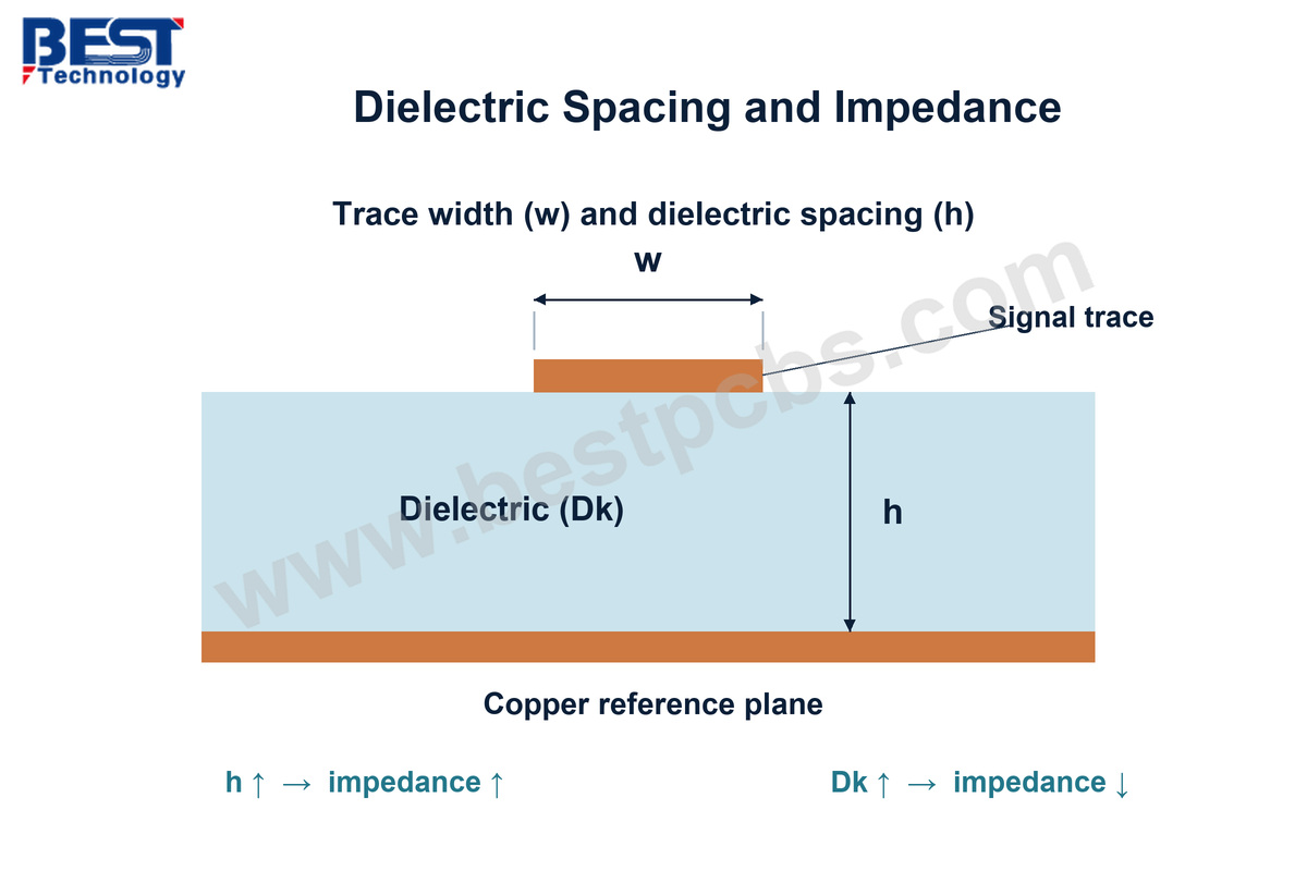
For a trace over a reference plane, the main relationships are:
- Greater dielectric spacing generally raises impedance when trace dimensions and material properties remain unchanged.
- Higher Dk generally lowers impedance for the same conductor geometry.
- Wider traces generally lower impedance, which allows a designer to compensate for some changes in dielectric spacing.
- Different core and prepreg constructions can require different trace widths, even when both belong to the same material family.
For a 50 Ω single-ended microstrip, a change in prepreg thickness can require a different trace width even when the material Dk stays the same. The example below uses Dk = 4.0, 0.035 mm copper, an uninterrupted reference plane, and no solder mask, calculated with the Hammerstad–Jensen quasi-static model including conductor-thickness correction.
| Finished trace-to-plane spacing | Trace width for approximately 50 Ω | Impedance if the original 0.380 mm width is retained |
|---|---|---|
| 0.150 mm | 0.279 mm | 41.8 Ω |
| 0.200 mm | 0.380 mm | 50.0 Ω |
| 0.250 mm | 0.481 mm | 56.9 Ω |
Increasing the spacing from 0.200 mm to 0.250 mm raises the calculated impedance by about 14% if the trace width stays unchanged. A material substitution that changes pressed spacing therefore needs an impedance recalculation, even when the overall board thickness remains 1.60 mm.
These are calculated comparisons, not production line-width recommendations; solder mask, etched trace shape, and the selected material’s Dk must be included in the final model. For 100 Ω differential pairs, the gap between the 2 traces also affects impedance.
For high-speed routing, the Dk value should correspond to the selected material construction and relevant frequency. A generic “FR-4 Dk” cannot describe every resin content or glass style. The fabricator’s proposed stackup and the routing geometry need to agree before the controlled-impedance traces are finalized.
What Affects the Cost of a Core and Prepreg Stackup?
Stocked core and prepreg combinations generally cost less to source than special-order constructions, while extra copper layers and repeated lamination cycles add manufacturing work.
- Standard material combinations: Commonly stocked core thicknesses and prepreg constructions usually offer easier sourcing than a special-order combination.
- Material grade: High-Tg, low-loss, or other specified resin systems can increase material cost when the electrical or thermal requirements call for them.
- Layer count: More copper layers add imaging, inspection, registration, and lamination work.
- Additional lamination cycles: Some HDI and buried-via constructions require repeated pressing and processing, increasing fabrication cost.
- Copper thickness and resin demand: Heavier inner copper creates deeper spaces for resin to fill and can require a different prepreg combination.
- Unusually tight thickness requirements: A narrow allowable thickness range can restrict the available materials and process choices.
For a conventional controller without demanding high-frequency requirements, a standard FR-4 construction may be sufficient. A low-loss laminate earns its additional cost when signal-loss requirements justify it.
How Does EBest Circuit Support Multilayer PCB Stackup Design?
EBest Circuit helps customers turn layer-count, board-thickness, and impedance requirements into a manufacturable core-and-prepreg stackup. Our PCB manufacturing capabilities cover FR-4 boards up to 32 layers, including HDI constructions.
For a multilayer project, our engineering review covers:
- Core thickness and layer spacing: We review the proposed dielectric dimensions against the overall board thickness and the signal/reference-layer arrangement.
- Prepreg construction: We consider glass style, resin content, copper distribution, and the number of plies needed for bonding and resin fill.
- Controlled impedance: We coordinate dielectric spacing and material Dk with trace width, finished copper thickness, and differential-pair spacing.
- Material and stackup changes: When available materials or copper distribution require a change, we raise an engineering query for customer confirmation before proceeding.
Our stackup and impedance guidelines explain the dimensions needed for this review. Customers can provide a finished stackup or ask us to propose a construction before routing the controlled-impedance traces.
We support prototype and volume orders, with PCB assembly services available for projects that also need populated boards.
What Information Do We Need for a PCB Stackup Quote?
We need the board files, layer requirements, material restrictions, and order quantity to quote a suitable core and prepreg construction. An existing stackup helps, but customers can also provide the electrical and mechanical targets for a proposed build.
- Fabrication data: Gerber files, drill files, board outline, and fabrication notes.
- Layer order: Copper-layer count and the intended signal, power, and ground arrangement.
- Finished thickness: Overall board thickness and its tolerance, plus any critical individual dielectric spacing.
- Copper requirements: Inner- and outer-layer copper weights or finished thicknesses.
- Impedance targets: Single-ended or differential values, tolerances, and the relevant layers or nets.
- Material requirements: A mandatory grade, Tg requirement, Dk/Df limits, or permitted alternatives.
- Order details: Prototype and production quantities, delivery requirements, and whether assembly is included.
For assembled boards, the BOM and component placement file complete the initial quotation package. If the stackup is still open, the required performance gives us a basis for proposing available materials without forcing an unnecessary custom construction.
FAQs About PCB Core and Prepreg
Is FR-4 the same as prepreg?
No. FR-4 describes a class of flame-retardant glass-reinforced epoxy material, while prepreg describes a partially cured material form. An FR-4 material system can be available as both cured copper-clad laminate and prepreg. The terms describe different aspects of the material, so “FR-4 versus prepreg” is not a comparison between mutually exclusive options.
Does a 2-layer PCB need prepreg?
A conventional 2-layer PCB usually does not need a separate prepreg bonding step during board fabrication. The fabricator starts with a 2-sided copper-clad laminate and forms circuits on its 2 faces. The laminate supplier used resin and reinforcement to make that core, but the PCB fabricator does not need to join additional circuit layers.
Can 2 thin prepreg plies replace 1 thicker ply?
Sometimes. 2 thin plies can achieve a similar finished dielectric thickness, but the combination must also supply enough resin to fill the adjacent copper pattern. Glass distribution and Dk may change, so equal nominal thickness alone does not establish an equivalent construction. The replacement should fit the required pressed spacing and electrical properties.
Can core and prepreg from different material families be combined?
Yes, compatible materials can form a hybrid stackup, including constructions that combine RF and conventional circuit layers. Their bonding behavior, cure conditions, and thermal expansion must suit the manufacturing process. Hybrid construction is useful when different parts of the board need different electrical properties, but arbitrary material mixing can create bonding or reliability problems.
Is a PCB core the same as a metal-core PCB?
No. In a conventional FR-4 stackup, the core is an insulating laminate supporting copper circuitry. In a metal-core PCB, the metal base—often aluminum—primarily spreads heat and supports the board. An insulating dielectric separates the circuitry from that metal base. These constructions serve different electrical and thermal purposes.
Does PCB prepreg have a shelf life?
Yes. Prepreg has a limited storage life because resin condition and moisture exposure affect its processing behavior. Storage temperature, humidity, packaging, and allowable storage time follow the specific material’s requirements. Fabricators track these conditions so the prepreg retains the resin flow and curing behavior needed for lamination.
Core provides the cured foundation for circuitry, while prepreg bonds the layers into a finished board. The right combination meets the design’s thickness, impedance, and manufacturing requirements without unnecessary material cost. For a multilayer PCB quotation, send your files and stackup requirements to sales@bestpcbs.com.
You may also like






Tags: 2116 prepreg, pcb core and prepreg thickness, pcb core material, pcb core vs prepreg, what is pcb prepreg