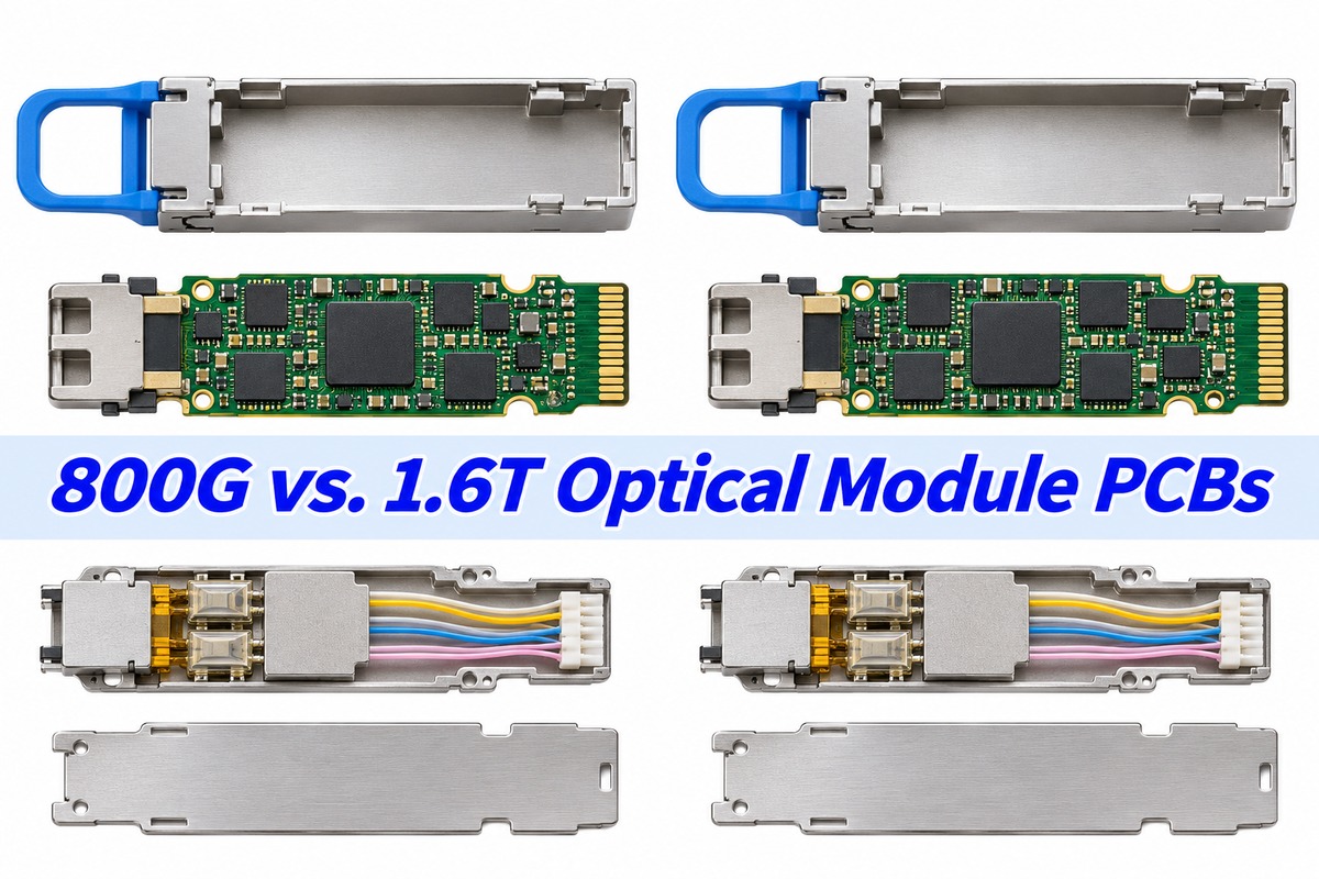
When comparing 800G vs. 1.6T Optical Module PCBs, start with the edge contacts, first via, and longest route. In an eight-lane QSFP-DD800 to QSFP-DD1600 upgrade, the lane count stays the same, but each host electrical lane moves from the 100 Gb/s class to the 200 Gb/s class. That changes the frequency range the channel must pass. The original laminate or layer count can stay if the new channel and mechanical checks pass.
Key Takeaways
- Compare the host electrical lane configuration, not just the aggregate rate. This article compares two eight-lane QSFP-DD implementations.
- Use the current paddle-card drawing before reusing the edge footprint. Model the contacts, trace neckdown and first via together.
- Keep the existing stackup only if the new loss and reflection checks pass across fabrication tolerances. A laminate upgrade cannot remove a via resonance.
- Recheck the power rails and package-to-lid contact against the new BOM and enclosure. Similar total power does not prove similar chip temperatures.
- Repeat the measurements that depended on the old interface, including fixture characterization and the installed thermal test.
800G vs. 1.6T Optical Module PCBs: Which Interfaces Are We Comparing?
The comparison below holds the module family and host lane count constant: QSFP-DD800 and QSFP-DD1600, each with eight host electrical lanes. The QSFP-DD MSA describes these electrical operating capabilities; the applicable interface specification sets the compliance frequencies, masks and test points. Optical configurations are outside this comparison.
| Design input | QSFP-DD800 | QSFP-DD1600 |
|---|---|---|
| Host electrical lanes | 8 × 100 Gb/s class | 8 × 200 Gb/s class |
| Per-lane PAM4 capability cited by the MSA | Up to 56 GBd | Up to 112 GBd |
| Nyquist frequency at those example rates | 28 GHz | 56 GHz |
| Module PCB edge | QSFP-DD800 paddle-card drawing | QSFP-DD1600 drawing with tighter tolerances on specified pre-wipe and signal pad dimensions |
Those baud rates are MSA capability examples, not universal test frequencies. A design using another lane configuration may change the number of traces rather than the rate per trace. Start with the exact interface and part drawings for the hardware you are building.
800G vs. 1.6T Edge Footprints: What Can You Reuse?
Use the old footprint as a reference, not as released artwork. QSFP-DD MSA Hardware Rev. 7.1 tightens specified pre-wipe and signal-pad tolerances for the QSFP-DD1600 paddle card. Start with the new drawing and compare the copper artwork and finished board dimensions to it.
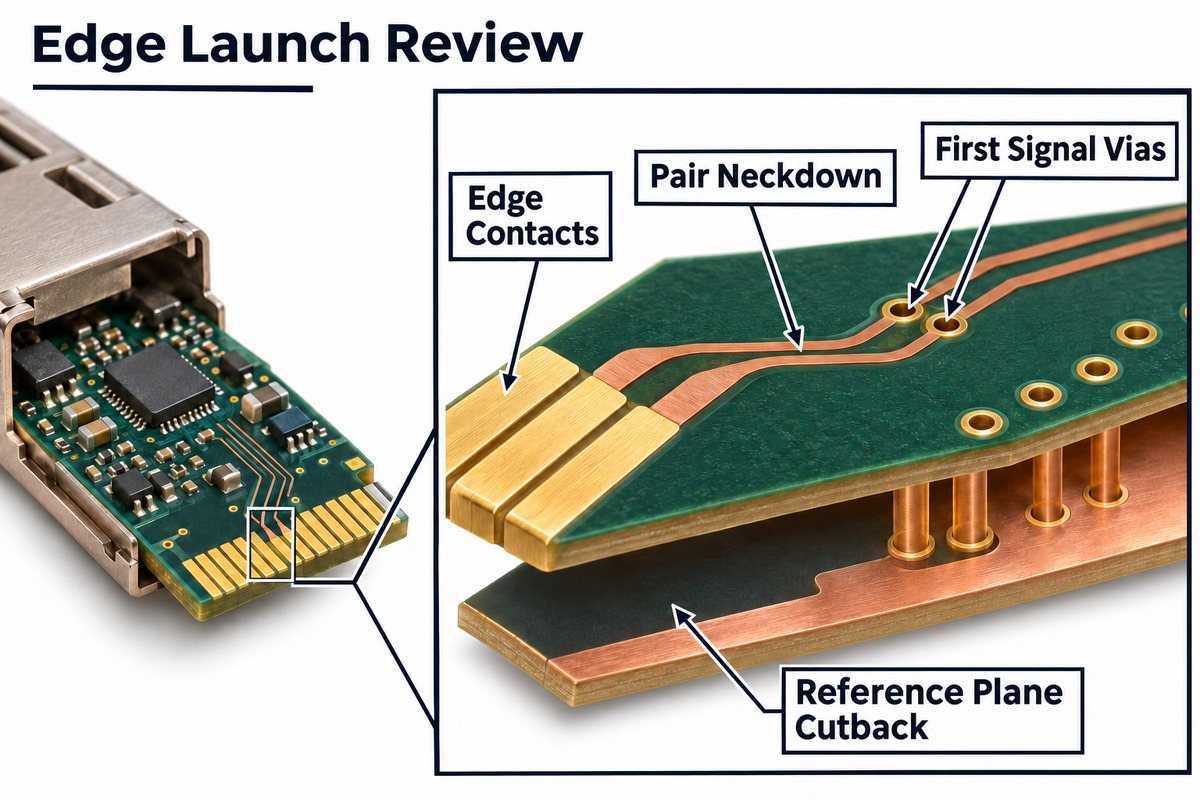
Model the launch with the mating contact, pad, trace neckdown and first via in the same structure. If the model shows a reflection at the edge, changing the laminate without changing the launch may leave the same problem. Before releasing the artwork, we can review the pad geometry, finished thickness and first via against the proposed controlled-impedance PCB stackup.
When Can the Laminate and Layer Count Stay the Same?
Keep them when the existing construction meets the new interface’s channel requirements at both nominal and manufacturing-limit dimensions. Test the longest route for loss and the most crowded route for coupling; they may be different lanes. Include the actual copper foil and dielectric thickness in both models.
If excess loss builds along the trace, first check whether you can shorten that route. If you cannot, compare a smoother foil or a lower-loss dielectric on a stackup the shop can actually build. If the problem is a sharp dip near a launch or a via, fix the transition first. The high-speed PCB materials guide explains the material variables; the decision here is whether changing them addresses the failure you measured.
Which Vias Need a Redesign?
Start with the vias that have the longest unused barrel, then check pad and antipad geometry and the ground return. For example, if a modeled via has a narrow loss dip near 45 GHz, a comparison that stops at 28 GHz will miss it. The dip sits below the 56 GHz Nyquist point in the 112 GBd example. This is a hypothetical result, not a measured failure or a compliance limit.
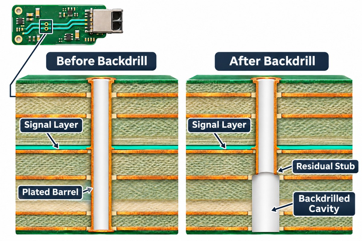
For the first layout review, mark the actual start and end layers of each critical via. Model the longest residual stub the fabricator can leave under its drilling tolerances. If that case fails, compare a different routing layer, backdrilling, or a blind via. A nominal backdrill depth is not enough to decide whether the remaining barrel is acceptable.
800G vs. 1.6T: What Changes in Pair Spacing and Skew?
Treat neckdowns and parallel runs as local problems first. A full-board spacing rule can miss a tightly packed section behind the connector or under a package. Compare coupling on those short sections before adding routing layers to the whole board.
Recheck skew in time, not just matched length in CAD. Two traces of equal length can experience different delay if their transitions or dielectric surroundings differ. Avoid adding tight serpentine bends beside the connector until you have checked whether the added coupling offsets the benefit of the length correction.
Can the Power and Cooling Design Carry Over?
Keep the 800G power and cooling design only if it fits the new devices and passes the same operating checks. Compare the new and old BOM rail by rail: voltage, transient load, sequencing and the current rating of the path to each device. Check voltage at the load, not only at the regulator output.
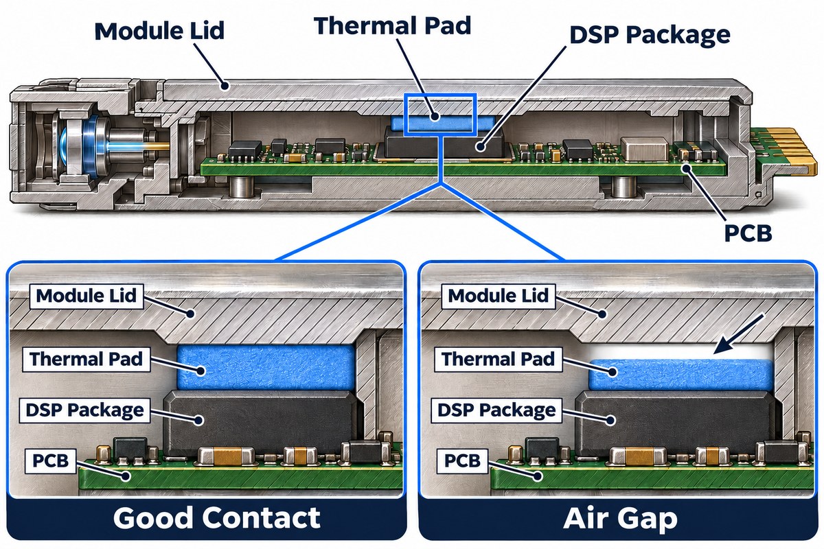
Then compare package height and the compressed thermal-pad thickness. A new package can leave a gap beneath a pad even when the module outline and total power look unchanged. Run the assembled module in the intended cage and airflow before committing to the existing lid or pad.
800G vs. 1.6T: Which Measurements Need to Be Repeated?
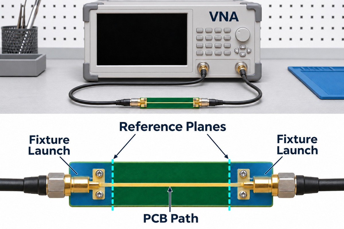
Repeat any measurement whose frequency range, reference planes or physical test path has changed. An impedance coupon can still confirm the fabricated pair geometry. It cannot qualify a new edge launch or show that the assembled electrical path meets its loss and reflection limits.
- Confirm the board build: finished thickness, contact dimensions, approved stackup and any specified residual-stub limit.
- Measure representative traces and transitions. Check that the fixture model and calibration cover the new test band before interpreting the results.
- Compare link behavior under the required supply and thermal conditions. Include the intended cage and airflow for the installed thermal check.
When the fixture itself has changed, recheck the measurement reference planes. Our PCB fixture de-embedding guide explains how to separate fixture effects from the board path.
What Is Worth Keeping from the 800G Design?
When reviewing 800G vs. 1.6T Optical Module PCBs, decide what to reuse based on the measured electrical path and the installed module. Keep the fabrication drawing conventions and test structures that still represent the new board. Keep the actual artwork only where the new interface, tolerance review and first-build measurements support it. If you already have a working 800G board, send the baseline stackup and the revised contact drawing to sales@bestpcbs.com. We can review which geometry needs to change before you release the new PCB.