






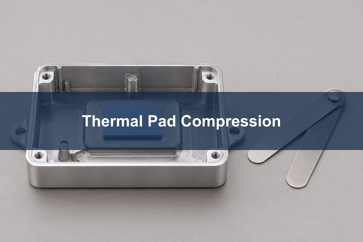
Choose a thermal gap pad for a PCB in an aluminum enclosure by checking the smallest and largest assembled gap. At one extreme the pad may not touch; at the other it may bend the board or overload the component. A higher conductivity rating cannot fix either problem.
Consider a hypothetical sealed industrial controller that transfers heat from a component to a machined aluminum boss through a compliant pad. The example shows how to convert the gap tolerance into a compression window, compare interface options, and decide what measurements are needed before releasing the assembly.
Aluminum PCB enclosure
An aluminum enclosure only helps cool a device when there is a usable heat path into the metal and from the metal to the environment. Start by marking the source, contact footprint, enclosure wall and exterior heat rejection. The enclosure and an aluminum-core PCB are different things; either may appear in the same assembly.
For the controller, the intended path is through the top of a component whose manufacturer allows that cooling arrangement. Check the drawing and applicable package guidance. If a component is designed to transfer most heat through an exposed underside pad, compare the board-to-case route rather than assuming the top case is a suitable contact.
PCB enclosure design guidelines
Define the gap between the actual mating surfaces with the PCB mounted on its production supports. Include component height, solder standoff, PCB position, boss location, relevant flatness and fastening tolerances. A dimension from the lid to the bare board is not the gap from the lid to the mounted component.
| Input | How to define it | Why it changes the decision |
| Gap, mm | Smallest and largest local separation in the closed build. | Determines contact and compression. |
| Pad thickness, mm | Nominal thickness and supplier tolerance. | Determines free height and assembled deflection. |
| Pressure and load | Supplier compression curve, loaded area and approved force limits. | Controls stress on package, board and fasteners. |
| Temperature limits | Component and enclosure limits under the specified duty and ambient. | Defines the actual release condition. |
Thermal pad thickness
With an illustrative 0.70–0.95 mm assembled gap and a 1.00 ± 0.05 mm free pad thickness, the least compression occurs with the thinnest pad at the largest gap. Here those dimensions are both 0.95 mm: there is no nominal squeeze in that worst-case combination. A build at the center of tolerance can look acceptable and still hide this failure.
Compare thickness options against both extremes and document the assumed tolerances. A nominal 1.20 mm pad with the same assumed ±0.05 mm thickness tolerance increases the minimum squeeze, but may increase load at the smallest gap. Do not choose it until the pressure and temperature evidence is available.
Thermal pad compression ratio
Compression ratio is (free thickness − assembled gap) divided by free thickness, expressed as a percentage when contact is achieved. For the 1.00 ± 0.05 mm example, the geometric envelope is 0% at 0.95 mm against a 0.95 mm gap and about 33% at 1.05 mm against a 0.70 mm gap.
For the 1.20 ± 0.05 mm option, the corresponding values are about 17% and 44%. These numbers are not recommended limits. Use the selected grade’s compression and loading data, and verify actual force and deflection if pad area or surface variation makes a uniform-pressure assumption unreliable. A metal stop or tighter tolerance may solve the problem more cleanly than another pad thickness.
Thermal pad vs thermal paste
Use a compliant pad when the assembly needs to bridge a designed gap. Consider paste for a thin, mechanically controlled interface between suitable mating surfaces; do not assume paste will bridge the controller’s millimeter-scale tolerance stack. A change of interface type also changes the manufacturing and rework plan.
| Option | Suitable condition | Verify before use |
| Gap pad | Variable gap with limited package or board load. | Compression window, contact area and pressure. |
| Thin paste interface | Close, controlled mating surfaces with defined clamping. | Application, bond line and service stability. |
| Revised boss or support | No pad can satisfy contact and load simultaneously. | Updated gap envelope and mechanical assembly fit. |
Thermal interface resistance
Use conductivity to estimate the bulk material contribution, not the complete interface. A simplified uniform layer has resistance equal to compressed thickness divided by conductivity times area. Using 0.80 mm, a 20 × 20 mm contact area and 3.0 W/(m·K), the bulk estimate is about 0.67 K/W. Henkel lists 3.0 W/(m·K) for one named gap-pad grade; the thickness and area here are hypothetical.
Contact resistance at both surfaces, uneven pressure and lateral spreading are excluded. Compare measured or supplier-characterized interface resistance at representative thickness and pressure. Even if a thicker pad guarantees contact, the added bulk resistance or higher force can make it the wrong choice.
Enclosure thermal analysis
Use the full path to decide whether improving the interface will reduce the temperature that matters. The package, pad, housing and outside environment can each limit performance, with some heat leaving by parallel paths. A cold enclosure alongside a hot component is a reason to check contact; a hot enclosure may indicate the system cannot reject enough heat externally.
For the controller, log actual dissipation, orientation and surrounding conditions rather than extrapolating from one open-bench test. Compare a poor-contact build and a verified-contact build with the same power and enclosure. See the aluminum enclosure and PCB integration guide for the broader fit and grounding questions.
PCB thermal testing
Verify the installed pad and the assembled thermal result independently. Inspect contact coverage by a method approved for the materials and build, record assembly settings, and measure the relevant component and enclosure temperatures under the specified operating modes. If using infrared measurements, account for emissivity and avoid inferring a junction temperature directly from a shiny enclosure reading.
Release only when representative builds cover the gap and load extremes, and the closed product satisfies the agreed temperature and mechanical limits. Retest if the support, pad grade, boss height or tightening sequence changes. Keep the insulation and grounding requirements separate: a thermal result cannot establish electrical safety.
FAQ
Should the pad thickness equal the measured gap?
Not by default. At that nominal condition there may be little or no compression. Check both thickness and gap tolerances and apply the selected material’s recommended conditions.
Can two thin pads replace one thick pad?
Do not assume equivalence. A stacked interface adds another contact boundary and may shift during assembly. Test the intended construction and obtain approval before changing it.
Does a soft pad guarantee low board stress?
No. The load also depends on deflection, area and support geometry. A large pad at a high compression can still create enough force to bend the board.
Can mounting torque tell me the pad’s contact pressure?
Not reliably by itself. Fastener friction, stops, enclosure stiffness and the force paths matter. Use a validated mechanical model or measurement when load is critical.
Does pad color identify its conductivity?
No. Use the supplier’s exact grade and current data rather than judging by color or appearance. Keep the part and thickness identifiers on the assembly record.
Is every thermal pad an approved electrical insulator?
No. Check the actual dielectric data and the complete insulation construction under the applicable requirements. Do not credit thermal material as a safety barrier by default.
Can I approve a build using one temperature snapshot?
Only if the accepted test plan calls for that observation and covers the relevant conditions. Otherwise record warm-up, equilibrium or duty-cycle behavior and the measurement locations.
What should I send to the board supplier?
Provide the board drawing, component and enclosure stack, contact location, permitted flatness and supporting assembly details. Keep the approved pad and load criteria with the product records.
References
- Henkel BERGQUIST GAP PAD TGP 3004SF product data
- Texas Instruments: thermal design of a top-side cooled package
Discuss the board-to-enclosure interface
For a Best Technology PCB or assembly review, send the board stack, contact geometry and inspection requirements to sales@bestpcbs.com.
You may also like






Tags: aluminum pcb, PCB enclosure, thermal management, thermal pads