





A power distribution PCB must carry continuous and peak currents without excessive voltage drop, overheating, or insulation failure. The challenge is not simply choosing thicker copper. Trace width, return paths, vias, terminals, and cooling conditions all affect how the finished board performs.
For custom high-current power distribution PCB projects, engineers need to know which copper structure will work, where manufacturing problems may occur, and how the assembly can be verified before production. EBest Circuit provides custom PCB manufacturing and PCBA assembly, supporting heavy-copper fabrication, component sourcing, prototypes, and volume production.
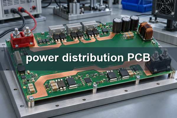
What Are Power Distribution PCBs Used for in High-Current Applications?
Power distribution PCBs route power from one or more sources to multiple electrical loads, often incorporating protection devices, switches, current sensors, and control circuitry. They are particularly useful when several high-current connections must fit within a compact assembly.
Typical applications include:
- Industrial automation and robotics: Distribute DC power to motors, actuators, controllers, and auxiliary equipment while handling changing load conditions.
- Battery energy storage systems: Connect power converters, protection devices, monitoring circuits, and DC distribution branches.
- Motor drives and power converters: Carry current between power semiconductors, capacitors, input connections, and output stages.
- Server and telecommunications equipment: Supply multiple electronic modules from a common power source while controlling voltage drop and heat generation.
- Vehicle electrical systems: Integrate power distribution, branch protection, and monitoring functions to reduce wiring complexity.
The PCB construction depends on the application. Moderate-current designs may use wide copper pours or parallel copper layers. Higher-current systems may need heavy copper, additional conductive layers, or integrated busbar structures.
The choice comes down to the available board space, operating current, temperature limits, electrical connections, and allowable power loss.
What Are the Key Design Requirements for High-Current Power Distribution PCBs?
High-current power distribution PCB design starts with the electrical and thermal requirements of each power branch. Specifying only the total input current is not enough to determine the appropriate copper thickness or conductor dimensions.
Before finalizing the layout, engineers should establish:
- Working voltage and load current: Define continuous current, peak current, peak duration, duty cycle, and simultaneous branch loading.
- Voltage-drop limit: Set the maximum permissible loss across the supply and return paths, including connectors and conductive transitions.
- Copper construction: Determine the proposed finished copper thickness, layer count, conductor width, and interlayer connections.
- Thermal conditions: Specify maximum ambient temperature, available cooling, permitted temperature rise, and sensitive component locations.
- Electrical insulation: Establish creepage, clearance, and insulation requirements according to the operating environment and applicable product standard.
- Power connections: Confirm connector ratings, contact resistance, finished-hole requirements, mounting method, and cable support.
The following example shows how these requirements might be defined for a 48 V DC power distribution PCB.
| Design parameter | Example specification |
|---|---|
| Working voltage | 48 V DC |
| Continuous branch current | 20 A |
| Peak branch current | 35 A for 200 ms |
| Maximum allowable voltage drop | 100 mV, including supply and return paths |
| Maximum ambient temperature | 40°C |
| Target conductor temperature rise | ≤20°C |
| Preliminary copper thickness | 70 μm finished copper |
| Preliminary conductor width | 10 mm |
| Supply and return conductor length | 100 mm each |
These are illustrative design conditions, not universal PCB design rules or guaranteed manufacturing specifications.
The final requirements should also define how the board will be evaluated. A design may meet its copper resistance target but still fail because of overheating at a connector, insufficient via capacity, or inadequate insulation spacing.
How Do Copper Thickness, Trace Width, and PCB Stackup Affect Current-Carrying Capacity?
Wider, thicker, and shorter copper conductors have lower electrical resistance. However, the current a PCB can safely carry also depends on temperature rise, layer placement, surrounding copper, and cooling conditions.
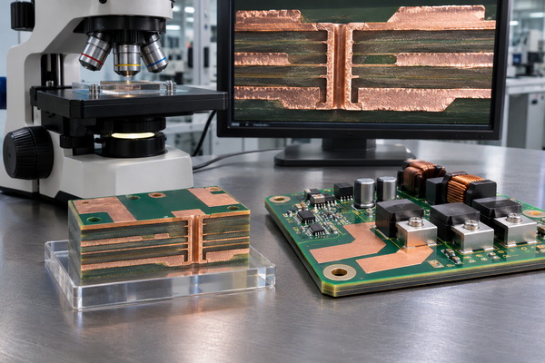
For a rectangular copper conductor, resistance can be estimated using:
R = ρL / (w × t)
Where:
- R: Conductor resistance (Ω)
- ρ: Copper resistivity, approximately 1.68 × 10⁻⁸ Ω·m at 20°C
- L: Conductor length (m)
- w: Conductor width (m)
- t: Copper thickness (m)
Voltage drop is calculated using V = IR, while conductor power loss is P = I²R.
Consider the earlier example: a 20 A branch with 100 mm supply and return conductors, each 10 mm wide and 70 μm thick.
At 20°C, the calculated values are:
- Resistance of each conductor: Approximately 2.4 mΩ
- Total supply-and-return resistance: Approximately 4.8 mΩ
- Voltage drop at 20 A: Approximately 96 mV
- Total copper power loss: Approximately 1.92 W
The design allows a maximum drop of 100 mV, leaving only 4 mV for additional losses at 20°C.
Copper resistance increases as temperature rises. If both conductors reach 60°C, the estimated copper-only voltage drop increases to approximately 111 mV, exceeding the specified limit.
This calculation assumes uniform conductor dimensions and temperature. It excludes connector resistance, solder joints, vias, and other losses. It also does not establish a safe continuous-current rating.
Several changes can reduce conductor losses:
- Increase trace or copper-pour width where board space permits.
- Use thicker finished copper when wider conductors cannot provide sufficient cross-sectional area.
- Add parallel conductive layers with properly designed current-sharing connections.
- Shorten the supply and return paths to reduce resistance without necessarily increasing copper weight.
- Consider copper inlays or busbars where conventional copper routing cannot meet the electrical and mechanical requirements.
Stackup selection also affects heat dissipation. An external copper layer has different cooling conditions from an internal plane, while parallel conductive layers need adequate plated connections to share current effectively.
IPC-2152 provides guidance for evaluating conductor geometry, current, and temperature rise. Its methods should be applied to the actual PCB construction rather than used as a universal width-to-current rule.
How Can Voltage Drop, Overheating, and Insulation Risks Be Reduced in Power Distribution PCBs?
Voltage drop and overheating are often concentrated at narrow copper sections, layer transitions, and power connections—not across the widest areas of a copper plane. These locations deserve particular attention before the layout is released for manufacturing.
- Voltage drop at narrow power paths: Check copper neck-downs around fuses, MOSFETs, connectors, and current-sensing components. Where possible, widen the conductive path or reduce its length while preserving the required circuit function.
- Heat buildup around vias: Review finished hole-wall copper, via placement, and the current entering or leaving each layer. A larger copper plane will not prevent overheating if current must pass through an undersized transition.
- Connector and terminal heating: Account for contact resistance, solder-joint resistance, connector current rating, and cable loading. High-current connectors may need additional mechanical support to prevent damage to PCB pads and solder joints.
- Uneven thermal distribution: Avoid concentrating power losses near temperature-sensitive components. Use suitable copper distribution, thermal interfaces, or cooling arrangements where needed.
- Insufficient insulation spacing: Set creepage and clearance according to working voltage, transient conditions, pollution degree, insulation requirements, material group, altitude, and applicable equipment standards.
- Overload and fault conditions: Coordinate protection devices so fault current is interrupted before it causes unacceptable heating or damage to the conductive path.
Creepage and clearance serve different purposes. Clearance is the shortest air distance between conductive parts; creepage is measured along an insulating surface. Neither should be selected from working voltage alone.
Once the PCB is assembled, voltage drop and temperature should be checked under the specified load and cooling conditions. Measurement locations should include connectors, layer transitions, narrow copper regions, and other potential hot spots.
How Are Custom Power Distribution PCBs Manufactured and Assembled?
Custom power distribution PCB manufacturing follows the normal PCB fabrication process but requires additional control of copper thickness, plated interconnections, and high-current component assembly.
The main production stages are:
1. Engineering Review and DFM
EBest Circuit reviews Gerber or ODB++ files, drill data, stackup, fabrication drawings, BOM, and assembly requirements.
For high-current designs, the review focuses on copper geometry, conductor spacing, layer transitions, terminal holes, solder-mask openings, and assembly access.
2. PCB Fabrication
The approved design proceeds through imaging, etching, lamination, drilling, plating, solder-mask application, surface finishing, and profiling.
Heavy-copper boards require particular attention to etching accuracy, copper balance, dielectric filling, and plated-hole quality.
3. Component Sourcing and Preparation
Power semiconductors, protection devices, connectors, current sensors, and other approved BOM components are prepared for assembly.
Component availability, substitutions, and customer-supplied materials are confirmed before the relevant assembly operations begin.
4. SMT and Through-Hole Assembly
SMT components are assembled using the appropriate placement and soldering processes. High-current connectors, large capacitors, and through-hole power components may require different soldering methods because of their thermal mass and mechanical structure.
5. Inspection and Verification
Bare PCBs undergo electrical and dimensional checks. Assembled boards receive applicable solder-joint and component inspections.
Functional, load, and thermal testing can be included when the customer supplies the required procedures and acceptance criteria and the testing scope is confirmed.
Completing the DFM review before fabrication helps prevent changes to copper geometry, hole dimensions, or terminal specifications after manufacturing has started.
What Are the Common Power Distribution PCB Manufacturing Challenges and Solutions?
Heavy copper, high-current interconnections, and large power terminals create several manufacturing problems that are less common in standard low-current PCBs.
The most important challenges and manufacturing solutions include:
- Thick copper makes fine traces and spacing difficult to maintain.
As copper thickness increases, etching becomes more demanding. EBest Circuit reviews trace width, spacing, pad geometry, and etch compensation against the selected finished copper thickness before production. - Insufficient via plating or distribution restricts current transfer.
Layer-to-layer current paths must account for finished hole size, hole-wall copper, via quantity, and placement. These features are reviewed together rather than relying on a single via current-rating assumption. - Uneven copper distribution increases lamination and flatness risks.
Large differences in copper coverage can affect resin filling, board thickness, and warpage. Copper balance and the proposed dielectric construction are checked during stackup review. - Large copper areas make terminal soldering more difficult.
Heavy copper draws heat away from solder joints. The assembly process must provide sufficient heating and wetting without damaging the connector or nearby components. Soldering parameters and inspection criteria are selected for the actual assembly. - High-current connectors place mechanical stress on PCB pads.
Heavy cables, tightening forces, and vibration can damage connections. Mounting support, strain relief, finished holes, and connector installation requirements need to be addressed before assembly.
These issues are easier to resolve before production than after a prototype fails inspection or requires rework. Providing complete copper, connector, and mechanical specifications during DFM reduces the risk of costly manufacturing changes.
Why Choose EBest Circuit as Your Power Distribution PCB Manufacturer?
EBest Circuit combines high-current PCB fabrication and PCBA assembly with manufacturing review before production. For OEM buyers, this means copper construction, terminal installation, and assembly requirements can be evaluated together instead of being handled by separate suppliers.
EBest Circuit can provide:
- Heavy-copper PCB manufacturing: Standard FR-4 capabilities include 0.5–5 oz inner copper and 1–5 oz outer copper. Special-process options up to 20 oz are available for engineering review.
- Manufacturing feasibility review: Copper spacing, plated holes, layer construction, board thickness, and high-current terminal requirements can be checked before fabrication.
- PCB fabrication and assembly coordination: Bare boards, component sourcing, SMT, and through-hole assembly can be managed under an agreed manufacturing scope.
- Prototype and volume production: Customers can begin with engineering samples and move toward repeat production using approved manufacturing documentation.
- Project-specific quality requirements: Inspection records, electrical testing, and applicable functional tests can be included according to the agreed acceptance requirements.
Heavy-copper capability must always be evaluated together with spacing, board size, layer count, and hole construction. A 20 oz copper capability does not mean every 20 oz design can be manufactured with standard PCB trace dimensions.
What Power Distribution PCB Manufacturing and Assembly Services Does EBest Circuit Offer?
EBest Circuit supports PCB fabrication only, PCBA assembly only, or combined manufacturing and assembly for custom power distribution boards.
Customers can request the following services according to their project requirements:
- Custom PCB fabrication: Multilayer FR-4 boards with specified finished copper thickness, stackup, board thickness, surface finish, and mechanical features.
- High-current PCB manufacturing: Heavy-copper construction and special conductor structures, including busbar PCB options where appropriate.
- SMT and THT assembly: Assembly of power semiconductors, passive components, protection devices, connectors, and through-hole power components.
- Component sourcing: Turnkey, partial-turnkey, and customer-supplied material arrangements.
- Prototype and production orders: Engineering samples, pilot builds, and repeat production using approved files.
- Inspection and testing: PCB electrical testing, assembly inspection, and agreed functional or load verification.
For a combined manufacturing and assembly order, the quotation should identify which materials, inspection activities, test fixtures, and documentation are included. This is especially important when the board contains specialized connectors or requires high-current load verification.
How Does EBest Circuit Ensure Power Distribution PCB Quality and Reliability?
Power distribution PCB quality depends on correct conductor fabrication, reliable solder joints, and inspections matched to the finished board’s operating requirements.
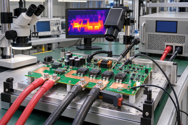
EBest Circuit applies manufacturing and assembly quality controls according to the approved project specifications.
For bare PCB fabrication, inspection can cover:
- Open- and short-circuit electrical testing.
- Finished thickness, hole dimensions, and critical conductor geometry.
- Surface finish and solder-mask quality.
- Hole-wall plating and cross-section analysis where required.
For PCBA assembly, applicable inspection methods include:
- SPI: Solder-paste deposition before component placement.
- AOI: Visible component placement and soldering defects.
- X-ray: Hidden solder joints where optical inspection is insufficient.
- Through-hole inspection: Solder wetting, visible joint quality, and specified terminal assembly requirements.
These checks identify manufacturing and assembly defects, but they do not independently establish the finished PCB’s current-carrying capacity.
When load testing is required, the agreed procedure should define applied voltage, current, test duration, cooling conditions, measurement locations, acceptable voltage drop, and temperature limits.
EBest Circuit lists ISO 9001:2015 among its quality-management certifications. Customers can request the applicable certificate and manufacturing documentation to verify the certified entity, production scope, and validity.
Case Study: Four-Layer Heavy-Copper PCB for Industrial Power Control
A four-layer heavy-copper PCB project for an industrial power-control module illustrates the manufacturing problems that can arise in compact, high-current power paths.
Project Background
The customer was developing an industrial power-control module containing MOSFETs, high-current terminals, protection circuitry, and control components.
The board had limited space for current routing and needed prototype validation before batch production.
Project Requirements and Challenges
The main requirements were stable current delivery, reduced local heating, reliable layer-to-layer connections, and consistent SMT assembly.
During engineering review, EBest Circuit identified narrow high-current paths, insufficient via distribution near selected current transitions, and copper-balance concerns affecting manufacturability.
EBest Circuit’s Manufacturing Solution
The manufacturing review covered:
- Widening critical copper paths.
- Increasing via distribution near high-current transitions.
- Reviewing copper around MOSFETs and power terminals.
- Improving copper balance across the four-layer construction.
- Checking solder-mask openings and assembly conditions.
- Controlling heavy-copper fabrication and PCB inspection.
After confirming the revised construction, EBest Circuit produced the engineering prototype and completed the required fabrication and assembly inspections.
Project Results
The prototype passed the reported PCB electrical testing, visual inspection, and assembly inspection. Customer-side prototype validation was completed before the project proceeded toward batch production.
The project shows why copper distribution, layer transitions, and assembly conditions need to be reviewed together when manufacturing high-current boards.
What Affects the Cost and Lead Time of Power Distribution PCB Manufacturing?
Copper thickness, layer count, board dimensions, component availability, and testing requirements have the greatest influence on power distribution PCB cost and lead time.
| Cost or lead time factor | Why it matters | Practical cost-control method |
|---|---|---|
| Copper thickness and PCB layers | Heavy copper increases material use and makes etching and lamination more demanding | Use heavier copper only where electrical and thermal requirements justify it |
| Board size and panelization | Large boards and inefficient panel layouts increase material consumption | Review the board outline and panel arrangement before finalizing production files |
| Special conductor structures | Copper inlays and integrated busbars require additional materials and processing | Confirm whether conventional copper layers can meet the requirements first |
| Connectors and terminal assembly | Large power terminals may require additional tooling, soldering control, and inspection | Finalize connector part numbers and mounting requirements before quotation |
| Component availability | Long-lead components can delay an otherwise manufacturable PCB | Confirm approved alternatives and sourcing responsibilities early |
| Testing and documentation | Specialized load tests, fixtures, and reports increase preparation time and cost | Specify required tests, sample quantities, and acceptance criteria in the RFQ |
| Order quantity | Prototype setup costs are spread across fewer boards | Request prototype, pilot, and volume pricing using the same approved specifications |
For general turnkey PCBA projects, EBest Circuit publishes a planning reference of approximately 10–12 business days after the required files and purchase order are confirmed, subject to material availability and project complexity.
For certain 3–4-layer embedded busbar PCB constructions, a published fabrication reference is approximately 13–15 days.
Neither range should be treated as a guaranteed lead time for a custom heavy-copper power distribution PCB. Complex copper structures, component sourcing, special tests, and approval requirements may change the schedule.
International transportation and customs clearance are separate from manufacturing lead time. A reliable quotation should specify whether the required date is the factory shipment date or the final delivery date.
FAQs About Power Distribution PCB Manufacturing
Q1: Can I submit my PCB files under an NDA?
A1: Yes. Customers can request an NDA before providing confidential schematics, PCB layouts, or product documentation. The scope and terms should be agreed before transferring restricted information.
Q2: Can EBest Circuit use components supplied by the customer?
A2: Yes. Customer-supplied components can be included in an assembly project. The BOM, quantities, packaging, handling requirements, and responsibility for material shortages should be agreed before production.
Q3: What information is needed for high-current connector installation?
A3: Provide the connector part number, datasheet, recommended PCB hole pattern, mounting method, and relevant mechanical requirements. For press-fit or bolted connectors, additional tooling and installation requirements may need review.
Q4: What happens if a specified component becomes unavailable?
A4: EBest Circuit can review sourcing options and propose alternatives for customer approval. Substitutes must be checked for electrical ratings, mechanical compatibility, footprint, and assembly requirements before use.
Q5: Can engineering changes be made after the prototype is approved?
A5: Yes, but the revised files must be reviewed before implementation. Changes to copper geometry, connectors, components, or assembly requirements may affect existing materials, tooling, quotation, and production schedule.
Q6: How are repeat production orders controlled?
A6: Repeat orders should reference the approved PCB revision, stackup, BOM, assembly files, component substitutions, and applicable test requirements. This helps prevent differences between prototype and production builds.
Q7: How should heavy components and exposed terminals be protected during shipment?
A7: Packaging should prevent movement, impact, and damage to connectors, board edges, and exposed contacts. ESD protection, separation trays, terminal caps, and reinforced packaging can be specified as needed.
Q8: Can inspection reports be included with the shipment?
A8: Yes, when the required documentation is agreed as part of the order. Available project records may include electrical-test results, inspection reports, revision identification, and applicable traceability information.
Q9: Can a PCB design with nonstandard copper construction be quoted?
A9: Yes. Submit the complete stackup, finished copper requirements, conductor dimensions, drilled features, and target quantity. EBest Circuit can review manufacturing feasibility and identify any special-process requirements before quotation.
Request a Custom Power Distribution PCB Quote
Need a power distribution PCB that can carry high current without excessive voltage drop or overheating? EBest Circuit supports custom heavy-copper PCB manufacturing, SMT/THT assembly, component sourcing, and prototype-to-production orders for industrial power applications.
Send your Gerber files, BOM, stackup, copper requirements, quantity, required delivery date, and delivery location to sales@bestpcbs.com. Get a free DFM check and a project-specific quotation covering manufacturing feasibility, assembly, quality requirements, cost, and lead time.
You may also like



Tags: High-Current PCB, Power Distribution PCB, Power Distribution PCB Assembly, Power Distribution PCB Manufacturer