





A small chip on a ceramic PCB is not automatically acceptable or rejectable. Its location matters: a corner chip far from copper is a different problem from damage beside a conductor or beneath a clamp. Measure the affected feature and compare it with the agreed drawing before accepting the substrate.
What an Edge Chip Is
A chip is a local loss of material at an edge or corner. It may be visible after separation, handling or another operation. Record the first stage where it was observed, but do not assume that stage caused it.
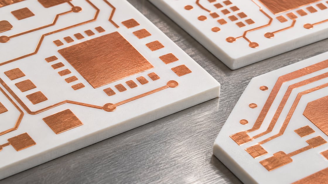
Chip vs Suspected Crack
| Observation | What it may indicate | What to do next |
| — | — | — |
| Local missing material | Chip | Measure its extent and position |
| Narrow line extending inward | Possible crack | Hold for appropriate examination |
| Edge texture repeats along separation line | Possible process texture | Compare with the approved edge reference |
| Copper is exposed or lifted | Affected metallization | Escalate the conductor condition separately |
Detailed Parameters to Record
| Parameter | Unit or record | Why it matters |
| — | — | — |
| Extent along edge | mm | Describes the affected length |
| Inward reach | mm from intended edge | Shows loss of clearance |
| Remaining gap to copper | mm | Supports the drawing check |
| Face and location | Top, bottom, corner or edge ID | Makes inspection reproducible |
| Suspected crack | Direction and visible extent | Triggers additional examination |
Use the Finished Outline as the Reference
Agree where the intended edge lies and how damage is measured relative to it. A chip’s visible width along the edge and its reach inward are different quantities. Mark the measurement direction and show the nearest relevant copper in the record.
Worked Example: Check the Gap to Copper
Suppose a conductor begins 0.45 mm from the intended outline and a local chip reaches 0.20 mm inward directly toward it. In this simple aligned example, 0.25 mm remains. If a hypothetical drawing requires 0.30 mm there, the part fails that requirement. For irregular damage, measure the actual shortest distance rather than subtracting unrelated dimensions.
Scribe-and-Break vs Full Separation
Scribing establishes a line for a later break. It is not the same as a process that fully separates the substrate during cutting. Kyocera’s ceramics catalogue illustrates a laser scribe geometry for its substrates; the example is not a transferable acceptance limit.
Check Both Faces and the Corner
A top view can miss damage visible on the underside or along the sidewall. Inspect the relevant faces and use adequate lighting and magnification. Keep the inspection method consistent when comparing a candidate part with the approved sample.

Treat a Suspected Crack Separately
Do not classify an inward line as ordinary texture solely because the part passes continuity. The observed line may need review by the responsible quality engineer using an approved method. Preserve the sample and document its location without attempting an unapproved repair.
Review How the Part Is Clamped or Supported
If the edge sits under a clamp, in a locating pocket, or against a fixture, a small geometry change can affect contact or positioning. Compare the actual damage location with the assembly interface. A corner outside the copper field is not necessarily outside the mechanical load path.
Check Whether the Pattern Repeats
Record the panel position and edge direction for each finding. Repeated damage near one separation feature can guide a review of the process or handling, but does not establish a cause by itself. Keep original photos and measurements rather than retaining only a summary count.
Put Inspection Criteria on the Drawing
Specify what to measure, where exceptions are prohibited and what triggers a hold. Include the inspection stage and sample condition. For the broader substrate design context, see the BestPCBs ceramic substrate design guide.
Release Against Evidence, Not Appearance Alone
Compare the actual dimensions and remaining clearances with the applicable limits. Where crack status, insulation or load support is uncertain, keep that question open until the responsible reviewer has enough evidence. A photograph is useful documentation, not automatic approval.
Discuss a Ceramic Substrate Requirement
Share the ceramic grade, outline and critical copper edge zones with Best Technology.
FAQ
Is every chip on a ceramic board a reject?
No universal rule applies to all constructions and uses. Evaluate the chip against the approved drawing, its location and the function of the edge. If the acceptance criteria do not cover the finding, obtain a documented disposition rather than relying on a visual impression.
Does passing continuity mean the chip is harmless?
No. Continuity tests the electrical path under defined conditions. It does not establish remaining clearance, mechanical support or absence of cracking. Check the feature that the drawing or assembly actually depends on, and keep the electrical result separate from the mechanical disposition.
How do I measure a chip at a rounded corner?
Use the intended contour from the drawing and the agreed inspection convention for that corner. Report the extent and location with a marked image where useful. Do not force an irregular feature into a straight-edge measurement if doing so hides the actual loss of clearance.
Can two chips of the same size have different outcomes?
Yes. One may be far from any functional feature while another is beside a copper pad, seal or clamp. Record the position and remaining distance to critical features as well as size. Apply the acceptance rule that belongs to that zone of the design.
Is a laser scribe mark automatically a defect?
No. A visible separation feature can be part of an approved process. Compare it with the drawing and reference sample, and look for additional damage that is not expected for that method. If the line appears to extend into the substrate, escalate it as a separate finding.
Can I use a phone photo for approval?
A photo can show the location and appearance, but perspective and lighting can hide depth or exaggerate size. Use it as supporting evidence. When approval depends on a numerical limit or suspected crack, use the measurement or inspection method specified for the part.
Should I sand the damaged edge before measuring it?
Do not alter the part without an approved disposition. Sanding changes the profile and may remove evidence needed to identify the finding. Document the as-found condition first, then follow any repair or rejection decision made by the responsible quality and engineering owners.
What goes into a ceramic edge inspection report?
Record the part revision, lot, ceramic grade, edge or corner identifier, observed extent and remaining clearance. Include the measurement method and representative images. Note separately whether a crack is suspected and who approved the disposition so that the decision can be traced later.
You may also like


Tags: ceramic PCB edge chipping, ceramic substrate inspection, copper edge clearance, laser scribing