A cavity PCB provides a lower mounting surface for components within part of the board. It can help a tall package fit beneath an enclosure cover while leaving the surrounding board at its original thickness. The recess also changes where component pads sit, which copper layers remain available and how the assembly equipment reaches the footprint.
EBest Circuit provides multilayer PCB fabrication, DFM support, component sourcing and PCB assembly. For a recessed-component project, a combined fabrication and assembly review can address the cavity geometry alongside the mounting process. Contact sales@bestpcbs.com to discuss your board stackup and component arrangement.
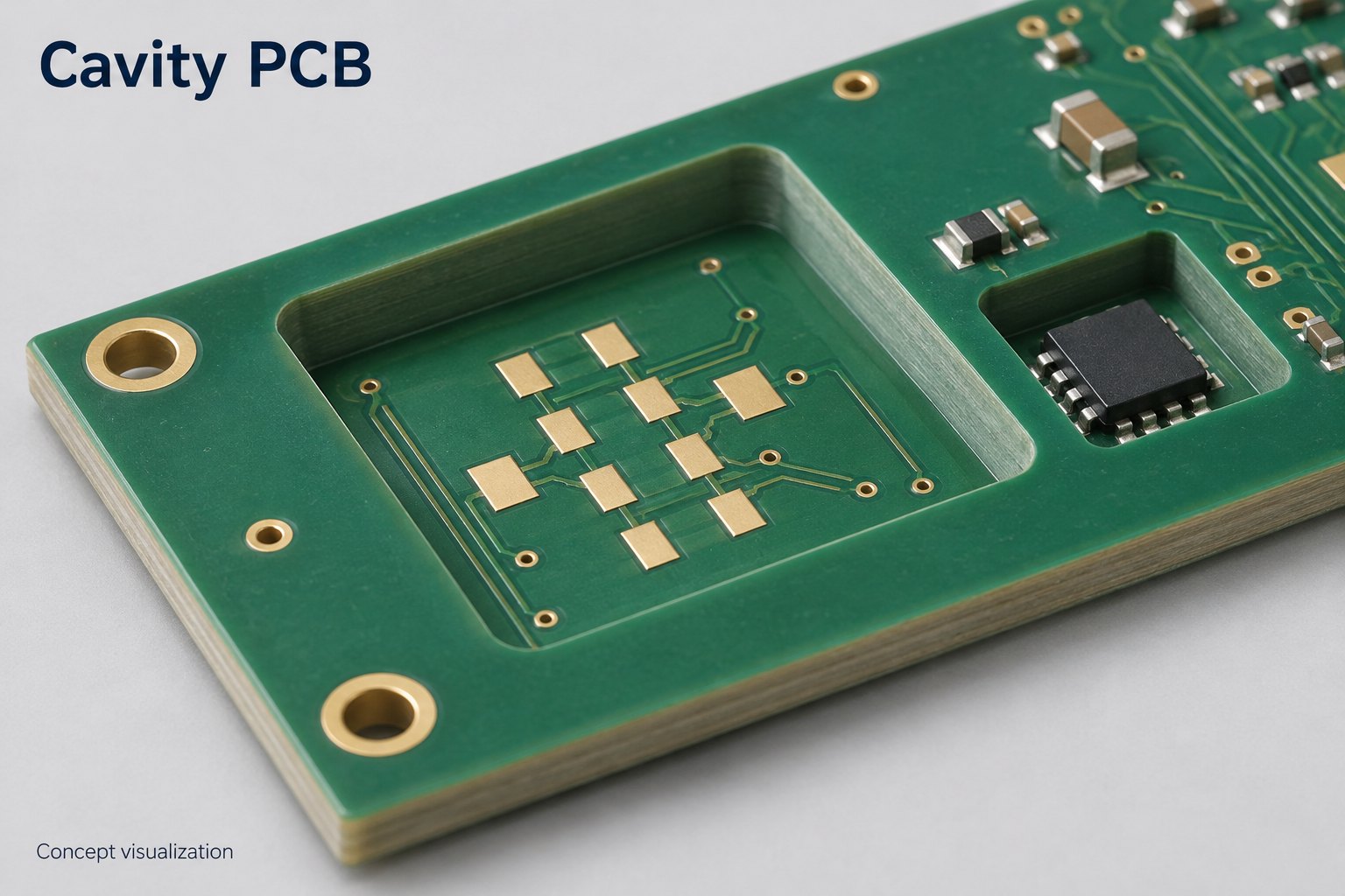
What Is a Cavity PCB?
A cavity is a local recess with a floor and board material beneath it. Depending on its construction, that floor can be bare dielectric, a copper surface or a circuit layer containing pads and traces.
| Feature | Cross-section | Typical use |
|---|---|---|
| PCB cavity | A recess that stops within the board thickness | Mount a component below the outer surface or expose an internal layer |
| Through-cutout | An opening through the full board thickness | Provide clearance through the board |
| Counterbore | A larger cylindrical recess around a smaller hole | Seat a screw head or washer below the surface |
For an SMD component mounted on the cavity floor, the exposed layer contains its footprint. The board must therefore preserve both the recessed shape and the copper features that connect the component to the circuit.
How Do Recessed Components Reduce Assembly Height?
The height saved above the board comes from lowering the component’s mounting plane. The package itself stays the same size.
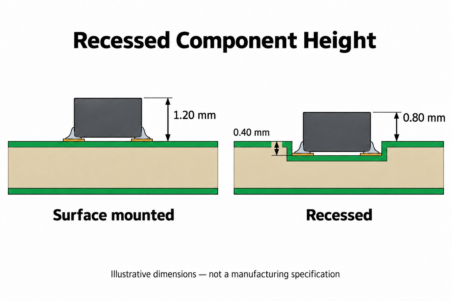
Here, assembled component height means the distance from the mounting-pad surface to the top of the installed component, including its soldered standoff. Cavity depth is measured from the surrounding board surface to that lower pad surface.
Component-top position relative to the board surface = assembled component height − cavity depth
For example, an assembled height of 1.20 mm and a recess depth of 0.40 mm leave the component top 0.80 mm above the board. A negative result would place it below the surrounding surface.
For the largest possible protrusion, use the maximum assembled height and the minimum recess depth. That upper position is what must fit beneath the enclosure cover, with the intended gap remaining.
This geometric example does not imply a manufacturing tolerance. Recessing one package also cannot reduce the enclosure height if a taller connector elsewhere still sets the limit. Increasing the board thickness to make room for the cavity can offset the height saved above it.
How Do Copper Floors and Plated Walls Change a PCB Cavity?
A bare pocket, a recessed footprint and a metal-lined cavity have different electrical structures. The distinction is where the copper remains and what it connects to.
| Copper arrangement | Structure inside the cavity |
|---|---|
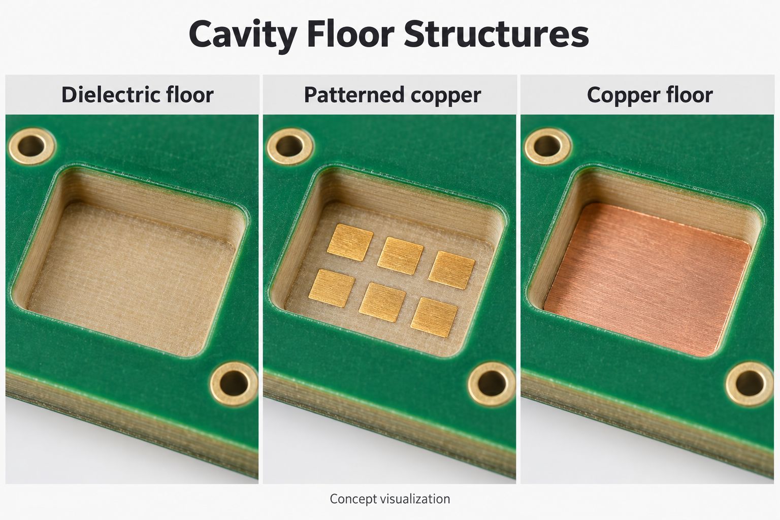
| No exposed copper | The floor is dielectric, with no conductive landing area for a soldered connection. |
| Patterned floor | Separate pads and traces form a component footprint or bonding pattern. Gaps between the copper features separate different electrical nets. |
| Continuous copper floor | A single conductive area can connect to ground or form part of a heat-spreading structure. |
| Plated walls | Metal extends along the sides of the recess and can connect to designated copper layers, such as ground. |
A patterned floor can coexist with plated walls. In that arrangement, signal pads remain separated from grounded wall metal; otherwise, the plating could join conductors that should be isolated. Floor pattern and wall plating therefore need separate definitions in the cavity design.
How Are PCB Cavities Manufactured?
Manufacturers form cavities through controlled-depth machining, lamination-based construction, laser processing or a combination of these methods.
Controlled-depth routing: A cutter removes material to a set depth. It leaves rounded internal corners and a machined floor. This process must stop before removing any copper or dielectric intended to remain below the pocket.
Lamination-based construction: Openings can be built into selected layers, with resin flow controlled around the cavity. Another approach forms a removable cap above a prepared inner layer; removing the cap exposes the recessed circuit pattern.
Laser processing: Laser energy removes dielectric to expose a metal surface or patterned circuitry. Near a patterned layer, controlled passes remove the remaining resin around copper features. Wall taper and floor cleanliness depend on the material and laser process.
For some constructions, routing removes most of the material and laser processing finishes the region near the target layer. This combines bulk removal with more selective exposure of the cavity floor.
What Limits Cavity PCB Design?
The main constraints are the material left beneath the cavity, the copper it approaches and the space needed around the component.
A deeper cavity leaves a thinner floor: For a simple one-sided pocket, minimum remaining thickness equals minimum board thickness minus maximum cavity depth. The remaining section must still contain the intended dielectric and circuitry. Increasing depth can remove that insulation or intersect an internal conductor.
A fixed depth is different from exposing a copper layer: A pocket dimensioned from the top surface is controlled by that surface reference. A cavity intended to expose an inner pad layer must also follow the layer’s actual position in the stackup. A nominal depth alone does not describe how to uncover the pads while preserving them.
Rounded corners can interfere with a square package: A routed pocket may match the package’s width and length along its straight sides yet still obstruct its corners. The cutter radius leaves material in those corners, so the package outline and cavity outline must be compared together.
Copper clearance extends beyond the visible opening: Traces, planes and vias on affected layers need separation from the finished wall and the possible machining variation. Moving surface copper alone does not protect a conductor buried beside the recess.
Package fit does not establish placement access: An opening that admits the component body may still obstruct the placement nozzle. Clearance must accommodate the tool as it lowers the package onto the recessed pads.
How Does Cavity Depth Affect SMT Assembly?
Cavity depth changes the vertical relationship between the stencil, pads and placement tool. The assembly process must reach the recessed footprint without being obstructed by the surrounding board.
Printing on a lower surface: A flat stencil resting on the outer board surface can leave a gap above recessed pads. A cavity-matched step stencil brings the printing region down to the footprint; the squeegee arrangement must also follow the stencil’s contour.
Placing at the recessed height: The placement machine must seat the component at the lower pad level. The nozzle’s shape and approach need enough clearance to avoid the walls during that movement.
In an AT&S cavity-assembly study, a step stencil and customized squeegee enabled printing, while paste-volume process capability decreased across the deeper test configurations. Placement and reflow were successful in that trial. The result shows that workable assembly and unchanged printing consistency are different claims; it does not establish a universal depth limit.
Can PCB Cavities Improve Cooling and RF Performance?
A cavity can shorten a heat path or change an RF structure, but those benefits come from specific connections and geometry.
Thermal path: Lowering a device can bring it closer to a conductive base or enclosure interface. Heat must still pass through the device attachment, intervening materials and the connection to the heat sink. An empty pocket supplies space; it does not supply that conductive path.
A buried copper coin PCB uses an inserted copper element to carry heat through part of the board. This is a different structure from leaving the recess open for a component.
RF structure: Replacing dielectric with an intentional air region changes the electrical environment around a signal or antenna. Grounded metal walls can also contribute to isolation. The resulting impedance and resonances depend on dimensions, dielectric distribution and ground connections, so an RF cavity belongs in the electromagnetic design.
Where shielding is the objective, an open metal-lined recess and a grounded enclosure with a lid have different boundaries. Sidewall plating alone should not be described as a complete shield.
Cavity PCB FAQs
Is a recessed component the same as a fully buried component?
No. A component in an open cavity can be reached from the open side. A fully buried component is enclosed within the board; reaching it would require opening or removing part of that structure.
Can cavities be made on both sides of a PCB?
Yes, in constructions that retain enough material between them. Where opposing pockets overlap, the remaining thickness is the local board thickness minus both recess depths. Their target copper layers must also remain intact.
Can one board contain cavities at different depths?
Yes. Separate cavities or stepped levels within a cavity can expose different layers. Each level has its own floor geometry; a footprint spanning two levels cannot be treated as a conventional flat mounting surface.
Can solder mask be applied inside a cavity?
Yes, some cavity processes support solder mask on a patterned floor. It can cover selected copper while leaving connection pads exposed. That floor coating is part of the fabrication sequence, rather than an automatic extension of the outer-surface mask.
Is a cavity outline in Gerber data enough to define the recess?
No. The outline defines its shape in the board plane, but not its vertical structure. A section view and fabrication notes identify the opening side, depth reference or target layer, remaining floor and any wall plating.
For your cavity PCB project, EBest Circuit can review the fabrication and PCBA requirements from your stackup, cavity section and component arrangement. Send these details to sales@bestpcbs.com to discuss the proposed build.