





micro usb pin configuration is the pin assignment used by a Micro USB connector to carry power, USB 2.0 data signals, identification, and ground. For most Micro USB 2.0 connectors, the five pins are VBUS, D-, D+, ID, and GND.
For engineers, buyers, and PCBA project teams, Micro USB pinout information is not only useful for cable wiring. It also affects connector footprint selection, solder joint reliability, ESD protection, functional testing, and how clearly the PCB assembly requirements should be communicated before production.
This guide explains the Micro USB 5-pin configuration, wiring color code, ID pin function, charging cable and data cable differences, and the PCB/PCBA checks that matter when a Micro USB connector is used on an electronic product.
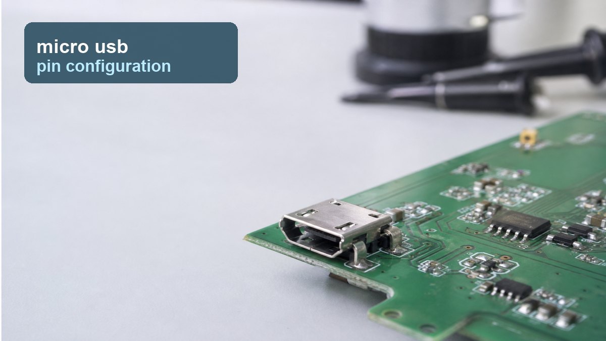
What Is the Micro USB Pin Configuration?
The Micro USB pin configuration is the order and function of the pins inside a Micro USB connector. A standard Micro USB 2.0 connector uses five pins: one power pin, two data pins, one ID pin, and one ground pin.
Basic Micro USB pin assignment:
| Pin | Signal | Common Function |
| 1 | VBUS | +5V power input |
| 2 | D- | USB 2.0 negative data line |
| 3 | D+ | USB 2.0 positive data line |
| 4 | ID | OTG identification pin |
| 5 | GND | Ground return path |
If you are comparing Micro USB with USB-A, USB-B, USB 3.0, or USB-C connectors, this related guide on USB port pin configuration can help you understand the broader connector family.
Micro USB Pinout Table: VBUS, D-, D+, ID, and GND
A Micro USB pinout table is usually the fastest way to confirm how each pin should be connected. The exact footprint should always be checked against the connector datasheet, because pad numbering, shell pads, mechanical pins, and orientation can vary by part number.
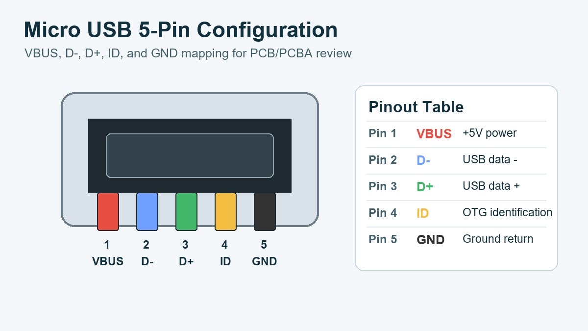
| Micro USB Pin | Name | Typical Connection | PCB Check |
| Pin 1 | VBUS | 5V input or charging power | Confirm power trace width, fuse, and protection needs. |
| Pin 2 | D- | USB 2.0 data pair | Route with D+ as a controlled pair where required. |
| Pin 3 | D+ | USB 2.0 data pair | Keep routing short and avoid unnecessary stubs. |
| Pin 4 | ID | OTG role identification | Confirm whether the design uses OTG or leaves ID unused. |
| Pin 5 | GND | Ground | Connect to a stable ground return and shield strategy. |
For PCB production, the important point is not only whether the signals are named correctly. The connector footprint, pad size, solder mask opening, shell retention pads, mounting style, and assembly notes must match the actual connector and the expected use environment.
What Are the 5 Pins in a Micro USB Connector?
The five pins in a Micro USB connector support power, data, device identification, and ground. Each pin has a different design concern on the PCB.
VBUS carries the typical 5V USB power line. In a charging or powered device, this pin may need protection, filtering, current control, or a clear connection to the power management circuit.
D- and D+ are the USB 2.0 differential data lines. These two traces should be reviewed carefully because routing imbalance, long stubs, poor return paths, or nearby noise sources can create signal quality problems.
ID is used for USB On-The-Go role detection. In many Micro-B device designs, the ID pin is not used. In OTG-related designs, its connection must follow the product design requirement.
GND is the ground return. It is also part of the connector reliability discussion because the connector shell, shield tabs, ESD strategy, and grounding approach can affect both electrical performance and mechanical robustness.
Micro USB Wiring Diagram and Wire Color Code
A common Micro USB cable color code is red for VBUS, white for D-, green for D+, and black for GND. The ID pin may not be connected in many standard cables. However, wire colors are not a substitute for verification, because cable suppliers and custom harnesses may not always follow the same color convention.
| Common Wire Color | Signal | Function |
| Red | VBUS | +5V power |
| White | D- | USB data negative |
| Green | D+ | USB data positive |
| Black | GND | Ground |
| Not always present | ID | OTG identification |
For a PCB or PCBA project, the cable and connector should be treated as part of the full assembly requirement. If the product depends on both charging and data transfer, the test plan should verify VBUS, D-, D+, and GND continuity instead of assuming the cable is data-capable.
USB-A to Micro USB Wiring: Charging Cable vs Data Cable
A USB-A to Micro USB cable may be built as a charging cable, a data cable, or a custom cable. A charging-only cable may connect VBUS and GND but omit usable D- and D+ data connections. A data cable should carry VBUS, D-, D+, and GND correctly.
This distinction matters during product validation. A device may charge normally but fail data transfer if the cable is charge-only or if D+ and D- are incorrectly wired. During PCBA functional testing, the test fixture and cable type should match the real product requirement.
For purchasing and production teams, this is also a BOM control issue. If the cable is bundled with the product, its function should be specified clearly. If the cable is only used for testing, the test cable should still be controlled so that false failures and false passes are reduced.
What Does the Micro USB ID Pin Do?
The Micro USB ID pin is mainly related to USB On-The-Go behavior. It helps determine whether a device should act as a host or a peripheral in designs that support OTG functionality.
In many Micro USB Type-B device designs, the ID pin is left unused or floating according to the product requirement. In OTG applications, the ID pin connection must be handled intentionally. It should not be guessed during PCB layout or assembly preparation.
From a manufacturing support perspective, EBest Circuit (Best Technology) can review approved PCB layout files, BOM information, connector footprints, and assembly notes for manufacturability. However, the final USB role design, protocol behavior, firmware, and compliance decisions should come from the product design team.
Micro USB Type-B Pinout vs Other USB Connector Types
Micro USB Type-B is commonly used on compact devices that need a small USB 2.0 connector for power and data. It should not be confused with Mini USB, USB 3.0 Micro-B, or USB-C.
| Connector Type | Typical Pins | Common Use |
| Micro USB 2.0 Type-B | 5 pins | Compact power and USB 2.0 data connection |
| Mini USB | 5 pins | Older portable devices |
| USB 3.0 Micro-B | More pins | Higher-speed USB 3.0 devices |
| USB-C | More complex pin set | Modern reversible USB connection |
When choosing a connector for a PCB project, the pinout is only one part of the decision. Mechanical strength, product thickness, insertion cycles, assembly method, supply availability, and test requirements should also be considered.
PCB Layout and DFM Checks for a Micro USB Connector
A Micro USB connector is a small mechanical and electrical interface, so PCB layout and DFM review are important before production. Even when the schematic pin names are correct, manufacturing issues can still appear if the connector footprint, pad design, or assembly notes are unclear.
Key checks include:
- Confirm the footprint against the exact connector datasheet.
- Check pad dimensions, solder mask openings, and stencil requirements.
- Review shell pads and mounting tabs for mechanical strength.
- Keep D+ and D- routing clean and balanced for the application requirement.
- Place ESD protection close enough to the connector when required by the design.
- Confirm connector orientation, board edge clearance, and enclosure fit.
- Define inspection and functional testing requirements before assembly.
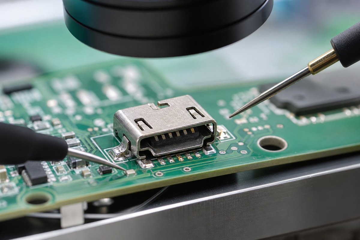
For prototype and small-batch builds, these details can save time because connector-related failures often appear during handling, repeated plugging, final enclosure fit, or functional testing. If your project needs quick validation, prototype PCB assembly support can help move the design from files to working boards faster.
Micro USB and USB Hub PCB Assembly Case Reference
A Micro USB connector is often part of a larger PCB or PCBA system, such as a USB hub board, compact control module, portable device, sensor interface, or embedded communication product. In these projects, the connector itself is only one detail. The full board must also meet impedance, mechanical fit, soldering reliability, BOM control, and delivery requirements.
For example, EBest Circuit (Best Technology) supported a Belgium customer with a USB hub-related rigid-flex PCB project. The board used a 3-layer rigid-flex structure, with an FPC area using ED copper and PI material, a rigid PCB area for component mounting, ENIG surface finish, gold finger bevel design, and 90-ohm impedance control. The order quantity was 100 pcs, and the related SMT assembly requirement was handled as part of the project workflow.
Project requirements:
- Application: USB hub-related electronic module
- Country: Belgium
- Board type: 3-layer rigid-flex PCB
- Key process: ENIG surface finish, gold finger bevel design, impedance control
- Quantity: 100 pcs prototype / small-batch order
- Assembly support: SMT assembly with material procurement support
Main challenges:
- Keeping the USB signal path stable with 90-ohm impedance control
- Matching the rigid-flex structure to the connector and product assembly space
- Reviewing the PCB production files before manufacturing
- Managing PCB fabrication and SMT assembly as one connected workflow
EBest Circuit solution:
- Reviewed the production files and stackup before fabrication
- Confirmed the rigid-flex PCB process requirements with the customer before production
- Supported PCB manufacturing, component sourcing, and SMT assembly
- Helped the customer move from engineering files to assembled boards for validation
This type of project shows why Micro USB pin configuration should not be treated as an isolated wiring detail. When a USB connector is used on a real PCB or PCBA, the supplier must also understand the board structure, impedance requirement, connector area, assembly process, and inspection points before production.
How EBest Supports Micro USB PCB and PCBA Assembly Projects
EBest Circuit (Best Technology) supports customized PCB and PCBA projects where Micro USB connectors are part of the product hardware. Our team can help engineers and buyers connect design files, BOM requirements, PCB fabrication, sourcing, assembly, and testing into one production workflow.
EBest Circuit supports Micro USB PCB and PCBA projects with:
- DFM review for approved PCB layout files.
- Connector footprint and assembly note review for manufacturability.
- PCB fabrication for prototype, small-batch, and production needs.
- Component sourcing support for connectors and related BOM items.
- SMT and suitable through-hole assembly processes when the connector or design requires them.
- Inspection and functional testing support based on the project requirement.
EBest does not replace the product design team for USB protocol design, firmware development, driver development, or compliance certification decisions. Instead, we support the manufacturability and production side of the project so the approved design can move into reliable PCB and PCBA production.
FAQs About Micro USB Pin Configuration
How many pins does a Micro USB connector have?
A standard Micro USB 2.0 connector has five pins: VBUS, D-, D+, ID, and GND.
What is the color code for Micro USB wires?
The common color code is red for VBUS, white for D-, green for D+, and black for GND. Always verify the actual cable because color conventions can vary.
What is the ID pin on Micro USB used for?
The ID pin is used for USB OTG role identification. In many Micro USB Type-B device designs, it may be unused or left floating according to the design requirement.
Can a Micro USB charging cable transfer data?
Not always. Some charging-only cables connect power and ground but do not provide usable D+ and D- data lines. A data cable should support VBUS, D-, D+, and GND connections.
What should be checked before assembling a Micro USB connector on a PCB?
Check the exact connector footprint, pad dimensions, solder mask openings, shell pads, connector orientation, D+/D- routing, ESD protection, inspection requirements, and functional test method.
In conclusion, micro usb pin configuration is simple at the pin table level, but it becomes more important when the connector is mounted on a PCB and used in a real product. A clear pinout, verified connector footprint, controlled BOM, careful assembly process, and practical testing plan can reduce connector-related failures before production.
EBest Circuit (Best Technology) supports PCB manufacturing, DFM review, component sourcing, PCBA assembly, and testing support for connector-based electronic projects. If you need help reviewing a Micro USB PCB or PCBA project, contact our team at sales@bestpcbs.com.
You may also like






Tags: micro usb pin configuration, micro usb pinout, micro usb wiring diagram