





A Solar Inverter PCB must carry high current, control fast switching, maintain safe isolation and remain stable under heat and outdoor electrical stress. A successful project therefore links circuit partitioning, stackup, copper geometry, component selection, assembly and testing from the first design review—not after a prototype fails.
What Is a Solar Inverter PCB and What Does It Do?
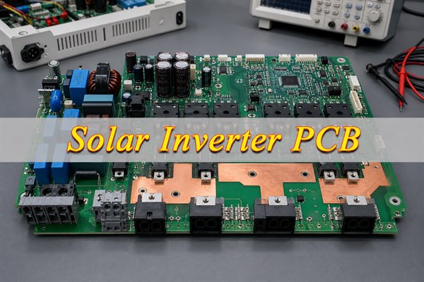
A solar inverter PCB is the electrical and physical platform that converts variable DC power from photovoltaic strings into controlled AC power. Depending on the architecture, one board may combine the DC input, MPPT converter, DC-link, inverter bridge, sensing, protection and communications. Larger systems often distribute these functions across a solar inverter power PCB and one or more control or interface boards.
The MPPT stage tracks the array operating point as irradiance and temperature change. The power stage switches MOSFETs, IGBTs or other devices, while the control section measures voltage, current and temperature and commands switching, protection and grid interaction. Communication interfaces such as CAN, RS-485 or Ethernet report status and receive settings.
Copper geometry carries current, dielectric spacing supports insulation, placement controls loop inductance and the laminate participates in heat flow. A correct schematic can therefore still produce EMI, unstable sensing, hot spots or switch damage when translated into a weak layout.
How Should Power, MPPT, Control and Communication Circuits Be Separated?
Separate circuits by energy level, noise sensitivity and isolation domain, while keeping every high-di/dt loop compact. The safest floor plan begins with functional zones before detailed routing. Power does not belong beside precision feedback merely because the available board area makes that placement convenient.
- PV input and protection: Place input connectors, fuses, surge protection, polarity protection and EMI filtering so surge and common-mode currents have a controlled path that does not cross the control ground.
- MPPT power stage: Keep the switching device, diode or synchronous device, inductor and local capacitor loop short. Place current sensing where it measures the intended path without sharing noisy copper.
- DC-link and inverter bridge: Position DC-link capacitors close to the bridge commutation loop. Use symmetrical power paths where parallel devices must share current.
- Gate drive: Place drivers close to their switches. Keep gate and return traces paired, away from switch nodes and separate from communication routing.
- Measurement and control: Route low-level voltage, current and temperature signals through a quiet region. Use Kelvin connections where the measurement must exclude load-current voltage drop.
- Communication interface: Keep connector-side transient protection near the connector, preserve differential-pair geometry where required and maintain the intended isolation barrier.
Do not create a single “quiet ground” label and assume the layout is quiet. Mark where current returns actually flow. A signal becomes vulnerable when its return path is forced around a split, through a switching-current region or across an isolation boundary. Review both normal operation and surge or fault-current paths before freezing placement.
What PCB Materials, Copper Weights and Stackups Are Suitable for Solar Inverters?
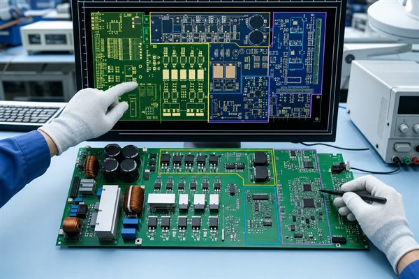
Material and stackup selection must follow voltage stress, temperature, current density, switching frequency and the required insulation system. High-Tg FR-4 is a common starting point, but a material name alone does not confirm comparative tracking index, thermal behavior, dielectric thickness or long-term suitability.
| Design Item | Selection Basis | Manufacturing Consideration | Release Check |
| Laminate | Maximum operating temperature, thermal cycling, CTI, voltage stress and loss at switching harmonics | Use a named material family or an approved-equivalent rule; do not specify only “FR-4” | Confirm datasheet values and the proposed construction |
| Copper weight | Continuous and peak current, allowable temperature rise, trace width, layer position and cooling | Thicker copper changes etching, minimum spacing, pad geometry, solder mask and planarization | Calculate each power path instead of applying one copper weight everywhere |
| Layer count | Power routing, control density, return paths, shielding and mechanical constraints | A mixed-signal multilayer stackup can provide reference planes while preserving high-current outer copper | Identify every plane, voltage domain and dielectric thickness |
| Dielectric spacing | Working voltage, transient category, pollution environment, altitude and insulation function | Core and prepreg choices must survive pressing tolerance and copper distribution | Review the finished stackup, not nominal prepreg data alone |
| Surface finish | Assembly process, storage, pad flatness, press-fit or connector needs and rework strategy | Finish choice affects solderability and exposed-pad protection, not the board’s current rating | Match the finish to component and assembly requirements |
Heavy copper is useful only when the geometry can be fabricated and assembled. Increasing copper may force wider conductor spacing and larger pads. It can also create solder-volume imbalance and local thermal mass. Use current-density and temperature-rise calculations, then confirm the selected construction with a DFM review before component placement is locked.
How Should a Solar Inverter PCB Layout Handle High Voltage, High Current and Switching Noise?
Handle high voltage with verified insulation spacing, high current with calculated copper geometry and switching noise with small commutation loops and controlled returns. These are related problems, but one layout rule cannot solve all three.
- Define voltage nets first: Classify PV input, DC-link, switch nodes, AC output, protective earth, isolated auxiliary power and safety extra-low voltage (SELV) circuits before routing.
- Calculate current paths: Size traces, pours, vias, terminals and bus connections for continuous current, overload, fault duration, copper thickness, ambient temperature and cooling.
- Minimize commutation loops: Place local capacitors and switching devices so the highest di/dt path encloses the smallest practical area.
- Control switch-node copper: Keep high-dv/dt nodes no larger than needed. Do not route sensitive traces beneath or beside them without an intentional shielding and return strategy.
- Use via arrays deliberately: Check via barrel capacity, current sharing, drill tolerance and thermal path. A large via count does not correct a narrow neck in the plane.
- Protect feedback routing: Use Kelvin sensing, paired routes and quiet reference regions. Filter placement should support the control loop rather than hide a noisy layout.
- Review gate loops: Keep gate-drive and return paths compact, maintain separation from power nodes and provide practical locations for damping components and measurement.
Clearance and creepage values must not be copied from a generic web table. They depend on working and transient voltage, material group, pollution degree, altitude, coating and the governing product safety requirements. Slots can increase creepage in a constrained area, but they also affect mechanical strength, contamination behavior and fabrication tolerance.
How Should Isolation, Grounding, EMC and Circuit Protection Be Designed?
Design isolation, grounding, EMC and protection together around normal, switching and fault-current paths.
- Define the isolation domains: Mark primary, secondary, chassis, protective earth and SELV regions on the schematic and layout. Classify every transformer winding, optocoupler, digital isolator, Y capacitor, connector shield, mounting point and test feature that crosses a barrier.
- Verify the complete insulation path: Calculate clearance and creepage from working voltage, transients, material group, pollution degree, altitude and insulation type. Check component packages, slots, exposed copper, fasteners and coating boundaries; an isolation symbol alone does not establish a compliant barrier.
- Control grounding and return current: Separate switching-current returns from sensing and communication references, then join domains only at intentional points. Do not route a sensitive signal across a plane split or force its return around a high-di/dt loop.
- Place EMC filters by current path: Keep common-mode and differential-mode filter inputs physically separated from their outputs. Place filtering close to the relevant connector or switching stage so noise cannot couple around the filter through copper, wiring or stray capacitance.
- Connect shields and chassis for high frequency: Use short, low-inductance connections and route discharge current away from logic references. Avoid long pigtails; confirm whether the shield is bonded directly, capacitively or through a controlled network.
- Coordinate overvoltage and surge protection: Select protective devices for the expected pulse voltage, energy, repetition and follow-on current. Check clamping voltage against semiconductor limits and coordinate the device with upstream fuses, breakers and product-level surge requirements.
- Control overcurrent, reverse polarity and temperature: Define detection time, shutdown behavior, fuse or breaker coordination and semiconductor safe operating limits. For battery-connected variants, verify reverse-polarity losses. Place temperature sensing at the component or heat-spreader location that represents the actual thermal limit.
- Protect external communication ports: Place ESD and surge devices close to the connector, minimize the discharge loop and keep the protected trace from recoupling into the unprotected side. Verify that protection capacitance and leakage remain compatible with the interface.
- Verify the finished design: Review the applicable edition and target market for IEC 62109-1, UL 1741 and related inverter certification standards, plus local grid requirements. Use approved insulation, surge, EMC and functional tests; PCB inspection alone cannot establish product compliance.
How Can Thermal Management Improve Solar Inverter PCB Reliability?
Thermal management improves reliability by controlling junction temperature, component exposure and temperature gradients from each heat source to ambient.
- Build a loss map: Estimate conduction, switching, magnetic, capacitor and connector losses under representative input, output and ambient conditions.
- Calculate junction temperature and derating: Combine measured case or board temperature with the applicable thermal-resistance model. Check normal load, overload and high-ambient conditions instead of relying only on a heatsink surface reading.
- Place heat sources intentionally: Keep power devices close enough for short electrical loops while leaving room for heat spreaders, airflow and assembly access.
- Design copper spreading: Use planes and local copper to reduce hot spots, but check electrical clearance, eddy-current behavior and the thermal bottleneck through dielectric layers.
- Engineer thermal vias: Specify diameter, pitch, fill condition and solder-control strategy. Verify that the via field connects to a useful internal or backside heat-spreading area.
- Control interfaces: Define flatness, insulation pads, thermal interface material thickness, mounting torque and component coplanarity where devices couple to a heatsink.
- Protect life-limiting components: Measure electrolytic capacitors, magnetics, optocouplers, relays and connectors as well as semiconductors. A nearby capacitor can determine service life even when the power switch remains within rating.
- Limit thermal gradients and cycling: Avoid placing hot power devices beside temperature-sensitive parts or mechanically constrained solder joints. Review heat-up, steady-state and cool-down conditions because repeated expansion can fatigue joints, vias and laminate.
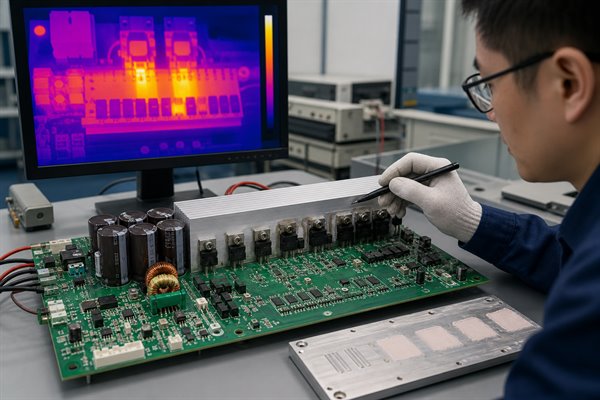
- Verify temperature measurements: Use thermal imaging to locate hot patterns, then confirm critical locations with thermocouples or attached sensors. Set emissivity correctly and account for reflections from exposed copper, metal hardware and heatsinks.
- Validate the enclosure: Test the assembled system at worst-case power, airflow, orientation and ambient conditions. A bench test with the cover removed is not representative.
What DFM Checks and Production Files Are Required Before Manufacturing?
A release package must define the board, assembly, programming and acceptance requirements well enough that manufacturing does not have to guess. DFM should identify questions before material purchase and stencil release, when changes are still controlled and inexpensive.
- Fabrication data: Supply Gerber or ODB++, NC drill files, board outline, layer order, controlled-impedance requirements, netlist and a fabrication drawing.
- Stackup definition: State finished thickness, copper weights, dielectric intent, material or approved-equivalent rule, surface finish and any CTI or insulation requirement.
- High-voltage notes: Identify voltage domains, keep-out areas, slots, coating exclusions and safety-critical dimensions that must not be altered during DFM.
- Assembly package: Provide BOM with manufacturer part numbers, approved alternates, centroid data, assembly drawings, polarity information and do-not-populate markings.
- Power-component details: Define press-fit, selective solder, mechanical fastening, thermal interface, torque and heatsink requirements where applicable.
- Programming instructions: Include firmware revision, programming connector, security or serialization rules and verification method.
- Test specification: Define test points, fixture interface, input limits, loads, pass/fail limits, safety precautions and required records.
- Change control: Use one released revision across fabrication, BOM, placement, firmware and test files; identify who can approve substitutions or deviations.
The DFM review should also check heavy-copper etching allowances, annular rings, hole-to-copper spacing, solder mask dams, thermal-pad paste apertures, polarized-component access and panelization. Use the contractually specified revisions of the applicable IPC board-design standards and assembly requirements rather than an undated internet rule. For a solar inverter PCB assembly, test access and safe discharge provisions should be designed into the board rather than added after the first build.
What Is the Solar Inverter PCB Manufacturing and Assembly Process?
The process must preserve design intent through material verification, PCB fabrication, controlled assembly, inspection, programming and functional test. Power boards often combine high thermal mass, small control components and large mechanical parts, so one generic SMT profile is rarely enough.
- Engineering review: Align stackup, copper, spacing, panelization, BOM, test coverage and mechanical requirements. Close technical questions under revision control.
- Material and component verification: Confirm laminate construction, copper foil, approved component sources, date or lot restrictions and alternates before release.
- PCB fabrication: Image and etch inner layers, laminate the stack, drill, metallize, plate, image outer layers, apply solder mask and finish, profile and electrically test the board.
- Bare-board inspection: Verify dimensions, holes, copper features, solder mask, surface finish and required coupons or microsections against the approved specification.
- Solder-paste printing and SMT: Control stencil design and paste deposit for fine-pitch control devices and thermal pads. Place and reflow components using an approved profile.
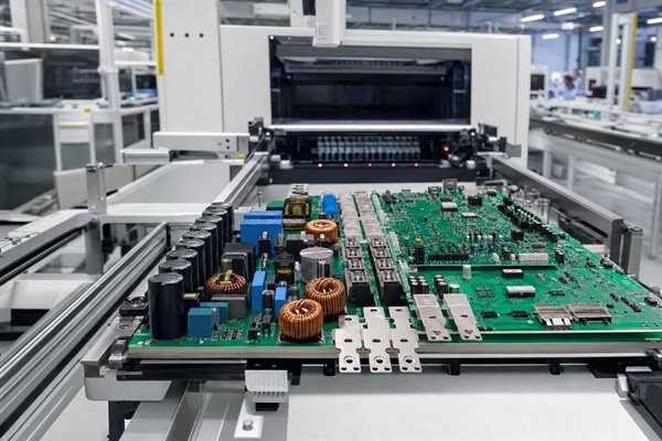
- Power-component assembly: Install large capacitors, magnetics, terminals, relays, semiconductors or heatsink hardware using the defined through-hole, selective-solder or mechanical process.
- Cleaning and protection: Apply the specified cleaning, ionic-cleanliness and conformal-coating controls only after compatibility and masking requirements are confirmed.
- Inspection and test: Complete visual inspection, AOI or X-ray where applicable, electrical tests, programming and functional checks with traceable records.
- Final configuration: Verify firmware, serial number, labels, mechanical interfaces and approved deviations before packaging.
Process sequencing matters. For example, installing high-mass hardware too early can obstruct inspection or expose sensitive parts to extra thermal cycles. The production plan should identify which joints need selective soldering, which bottom-terminated parts need X-ray and which assemblies require staged testing before high-voltage energization.
What Testing and Quality Control Are Required for Solar Inverter PCB Assemblies?
Testing must connect each design risk to a suitable inspection or measurement, a defined limit and a retained result. AOI cannot prove isolation, and a powered functional test cannot reveal every marginal solder joint. Coverage should combine process inspection, structural evidence and electrical performance.
- Incoming control: Verify critical power semiconductors, capacitors, magnetics, relays and safety components against approved sources and specifications.
- Solder-paste inspection: Use SPI where fine-pitch or bottom-terminated components make paste-volume control important.
- Optical inspection: Use visual inspection and AOI for polarity, presence, alignment, solder condition and visible damage.
- Hidden-joint inspection: Use X-ray for BGAs, QFNs, large thermal pads or other joints whose acceptance evidence is not visible.
- Bare-board electrical test: Confirm opens and shorts before assembly. Use appropriate netlist-based coverage for the released PCB.
- Low-voltage bring-up: Check shorts, auxiliary rails, programming and control behavior with current-limited supplies before applying hazardous energy.
- Functional test: Verify sensing, protection, gate commands, communication and control logic under defined loads and operating states.
- Safety-related test: Perform insulation resistance, dielectric withstand or protective-earth checks when required by the product test plan and governing requirements.
- Thermal and load validation: Measure critical temperatures and switching behavior at representative input, output, ambient and cooling conditions.
- Traceability: Record board revision, BOM revision, firmware, serial or lot identity, equipment, program revision, result and disposition.
Acceptance criteria should name the applicable assembly workmanship standard, product class, revision and customer additions. Product safety and performance limits must come from the approved product specification. For prototype builds, retain failure waveforms, thermal images and corrected-revision records so the next build starts from evidence rather than memory.
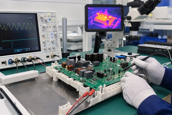
What Common Solar Inverter PCB Failures Occur and How Can They Be Prevented?
Most recurring failures trace back to excessive electrical stress, uncontrolled heat, parasitic switching behavior, weak insulation or inconsistent assembly. Prevention requires a cause-and-verification loop, not simply replacing the visibly damaged component.
| Failure Symptom | Likely Causes | Preventive Action | Verification Method |
| Power switch damage | Overshoot, poor gate control, excessive loop inductance, inadequate protection or thermal stress | Reduce loop area, tune gate network, coordinate clamps and confirm safe operating margin | Measure switching waveforms at representative voltage, current and temperature |
| Overheated copper or terminals | Narrow necks, weak via transfer, loose hardware, poor current sharing or undersized connectors | Calculate the complete current path and define assembly torque or connection controls | Use voltage-drop and thermal measurements under sustained load |
| False trips or unstable MPPT | Noisy sensing, poor return routing, common-mode coupling or unsuitable filtering | Use Kelvin sensing, controlled returns, local filtering and separation from switching nodes | Correlate raw sensor waveforms with control events across operating points |
| Isolation breakdown | Insufficient spacing, contamination, conductive debris, coating voids or transient overstress | Verify the insulation system, cleanliness, slots, coating process and surge coordination | Inspect critical spacing and apply approved safety-related tests |
| Cracked joints or intermittent connectors | Thermal cycling, heavy unsupported parts, board flex or unsuitable solder process | Add mechanical support, control solder profile and reduce local strain | Inspect joints and reproduce mechanical and thermal service conditions |
| Corrosion or leakage | Flux residue, moisture, ionic contamination or unsuitable coating coverage | Validate cleaning, drying, coating compatibility and environmental protection | Use cleanliness evidence and environmental testing tied to the product plan |
When a board fails, capture operating state, firmware, waveforms, temperature, load and environmental conditions before rework destroys evidence. Separate the initiating cause from collateral damage. A shorted switch, for example, may be the result of gate ringing or isolation failure rather than the original defect.
How to Choose a Solar Inverter PCB Manufacturer?
Choose a solar inverter PCB manufacturer by its ability to identify, control and document the risks in your actual design. Compare engineering evidence and production scope, not unit price alone.
- Verify fabrication capability: Require a DFM response against the proposed layer count, copper weight, dielectric construction, board thickness, hole structure, surface finish, heavy-copper spacing and high-voltage features. Published maximum values are not enough; the supplier must assess the complete stackup.
- Assess power-electronics experience: Ask how the team reviews current bottlenecks, via transfer, creepage-sensitive areas, switch-node geometry, thermal interfaces and mechanical support for magnetics, capacitors, terminals and heatsinks.
- Review material and component control: Confirm laminate identity, approved-equivalent rules, component sourcing channels, moisture-sensitive handling, date or lot restrictions and the approval process for alternate power semiconductors, capacitors, relays and magnetics.
- Check mixed-technology assembly: The supplier should control fine-pitch SMT, bottom-terminated parts, high-thermal-mass joints, through-hole or selective soldering, press-fit connections, mounting torque and thermal interface materials within one documented process plan.
- Match inspection to hidden risks: Verify when SPI, AOI, X-ray, bare-board electrical testing, dielectric or insulation tests, programming checks and functional tests are used. Each method should have defined limits and retained results.
- Confirm engineering communication: A capable manufacturer should identify conflicting files, ambiguous voltage domains, inaccessible test points, missing acceptance limits and unsafe bring-up conditions before material purchase or stencil release.
- Require traceability and change control: Confirm how PCB revision, BOM, firmware, test program, material lot, component lot, approved deviations, rework and final disposition are linked to delivered units.
- Evaluate prototype-to-volume continuity: Check whether prototype corrections are incorporated into controlled production files, fixtures and work instructions. A successful hand-modified sample is not a repeatable production baseline.
- Compare the complete production scope: Make sure competing proposals include the same fabrication, sourcing, assembly, programming, inspection, functional-test, documentation and packaging responsibilities. A lower price is not comparable when essential controls are excluded.
Custom Solar Inverter PCB Manufacturing and Assembly Case Study
This representative case study shows how EBest Circuit turns an incomplete solar inverter PCB package into a controlled manufacturing and assembly release. The value lies in the engineering actions and traceable outputs, not in unverified performance claims.
Project Background: The design combined a high-current inverter stage, isolated gate drivers, MPPT sensing, auxiliary power and an external communication interface on one assembly. Large capacitors, magnetics, terminals and power semiconductors created high thermal mass, while low-level sensing circuits had to operate beside fast-switching nodes. The initial Gerber data and BOM were available, but voltage domains, copper-current transitions, thermal interfaces, component substitution rules and production test limits were not fully defined.
Project Requirements: The customer needed a buildable stackup with controlled copper weights, clear separation between power and control regions, verified insulation boundaries and practical heat transfer to the enclosure. The assembly also required mechanical support for heavy components, controlled soldering of high-thermal-mass joints, revision-linked firmware, traceable component sourcing and a staged test method that would not apply hazardous bus voltage before low-voltage checks had passed.
Our Solution: EBest Circuit created one DFM question log covering high-current neck-downs, via-transfer points, creepage-sensitive features, switch-node area, gate-return routing, thermal-pad construction, solder access and test-point coverage. The stackup, fabrication drawing, BOM, placement data, assembly drawing, firmware and test specification were aligned to one revision. The assembly plan separated SMT reflow from through-hole or selective-solder operations and defined inspection for visible joints, hidden thermal pads and mechanically loaded connections. Bare-board electrical test, AOI or visual inspection, X-ray where required, current-limited bring-up and functional checks were assigned clear acceptance evidence.
Output Results: The release package contained an approved stackup, closed DFM questions, controlled fabrication and assembly files, approved component decisions, programming instructions and a documented inspection and test plan. The build team could identify what had to be checked, which result constituted acceptance and which revision applied to the delivered units. This created a repeatable baseline for prototype assembly and subsequent production orders while keeping any efficiency, yield, reliability or delivery claims subject to customer-approved measurements.
Why Choose EBest Circuit as Your Solar Inverter PCB Manufacturer?
EBest Circuit helps customers reduce technical handoffs, prevent avoidable rebuilds and move an approved prototype into repeatable production.
- Fewer handoff gaps: DFM, PCB fabrication, component sourcing, assembly, programming and testing can follow one controlled data package.
- Lower redesign risk: Power paths, isolation, thermal interfaces and assembly access are reviewed before material purchase and stencil release.
- Comparable production scope: Manufacturing limits, special-process items, inspection coverage and excluded work are clarified before the customer compares price and schedule.
- Better defect containment: Mixed SMT and through-hole assembly can be paired with AOI, X-ray and electrical or functional checks according to the actual joint and circuit risks.
- Repeatable follow-on orders: Approved BOM changes, firmware, deviations, test programs and prototype corrections are transferred into a revision-controlled production baseline.
- More credible delivery planning: The committed schedule is based on material availability, engineering closure, fabrication complexity, assembly scope and test readiness—not an unsupported fast-turn promise.
FAQs About Solar Inverter PCB Boards
Q1: Can the same solar inverter PCB design be reused at a higher power rating?
A1: Not without a complete electrical, thermal and safety review. Higher power can change RMS and peak current, semiconductor loss, magnetic design, capacitor ripple, connector loading, copper temperature, protection settings and cooling demand. Revalidate the power stage, control limits, firmware and product compliance before releasing a higher-rated variant.
Q2: Is a solar hybrid inverter PCB different from a grid-tied inverter PCB?
A2: A hybrid design usually adds battery-side power conversion, bidirectional energy flow and additional protection and communication states. That can change current paths, connector count, control complexity, thermal loading and test scenarios. The board architecture must follow the complete energy-flow diagram rather than the product label alone.
Q3: What data should be controlled for custom magnetics used on the board?
A3: Control the electrical design, insulation construction, mechanical drawing and approved source together. Record turns ratio, inductance or energy-storage target, core and gap, winding wire, insulation system, temperature class, hipot requirement, pinout and dimensional limits. Incoming inspection should verify the characteristics that can affect switching, safety and mechanical fit.
Q4: How should high-current terminals and crimped cables be validated?
A4: Validate the complete connection, not only the PCB pad or terminal current rating. Define conductor size, crimp tool and inspection method, insertion or fastening torque, strain relief, contact resistance and allowable temperature rise. Use representative current and environmental conditions, then retain results that link the cable, terminal, fastener and board revision.
Q5: Who should own and maintain the production test fixture?
A5: Ownership, revision control and maintenance responsibility should be agreed before fixture development starts. The agreement should cover design files, replaceable wear parts, calibration or verification intervals, software version, storage, repair approval and transfer rights. Without these controls, a repeat order may use a fixture that no longer matches the released board or test limits.
Q6: When should a prototype revision be frozen for pilot production?
A6: Freeze the revision only after open engineering questions, approved rework and test limits have been incorporated into controlled files. Confirm that fabrication data, BOM, placement, drawings, firmware and test instructions share the same revision baseline. A successful hand-modified prototype is not a production release until every modification is documented and repeatable.
Q7: How should moisture-sensitive components be handled before assembly?
A7: Follow the component’s declared moisture-sensitivity level, floor life and reflow requirements. Record the sealed-pack condition, humidity indicator card result, opening time and remaining floor life. If exposure exceeds the approved limit, use the component manufacturer’s baking and handling instructions; uncontrolled baking can damage packaging, finishes or tape-and-reel materials.
Q8: What causes audible noise in an assembled solar inverter board?
A8: Magnetics, ceramic capacitors, mechanical resonance and control behavior are common sources. Investigate operating point, switching or modulation frequency, mounting, magnetic construction and waveform stability. The PCB can contribute through weak support, pulsed current paths or coupling, but the sound source should be measured before redesign.
Q9: How should spare solar inverter PCB assemblies be stored for field service?
A9: Store service boards in sealed ESD-safe packaging under controlled temperature and humidity. Protect connectors, coated surfaces and thermal interfaces from contamination or compression. Record packing date and storage conditions, follow component moisture and shelf-life limits, and define visual or electrical reinspection before an aged spare is installed.
Q10: How should a golden sample be controlled?
A10: A golden sample needs an approved identity, purpose, storage condition and expiration or review rule. State whether it represents appearance, mechanical fit, programming, functional response or test-fixture correlation; one sample may not cover every purpose. Seal or label it against unauthorized rework, link it to the released revision and periodically confirm that it still represents current acceptance criteria.
If you need custom Solar Inverter PCB design support, prototype fabrication, PCB assembly or production review, send your Gerber/ODB++, BOM, quantity, stackup, assembly drawings, programming method and test requirements to sales@bestpcbs.com. EBest Circuit will review the manufacturing risks, clarify the open requirements and prepare a project-specific quotation.
You may also like





Tags: solar inverter PCB assembly, solar inverter PCB design, solar inverter PCB manufacturing, solar inverter PCB testing