





Reliable access control starts at the field-wiring boundary. A door access control PCB must make every credential decision, lock command and alarm input predictable. Reader compatibility, lock current, fail-safe behavior, communication security, surge protection, power-fail recovery and production testing must be designed as one system.
EBest Circuit supports PCB design, fabrication and assembly, including prototyping and component sourcing, for custom access-control hardware. A useful quotation starts with the door count, reader protocol, lock type, input voltage, network interface, enclosure limits, firmware responsibility and acceptance-test requirements.
What Is a Door Access Control PCB?
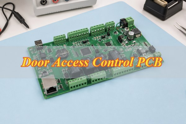
A door access control PCB makes and executes entry decisions. It receives credential and door-status signals, applies access rules and switches the locking hardware. It may operate as a standalone panel, an intelligent network controller or an interface board connected to a larger security platform.
A door access control PCB normally connects readers, request-to-exit devices, door-position contacts, tamper switches, alarms and electric locks. Its firmware decides whether a credential and event state permit entry, records the event and drives a relay or protected solid-state output.
- Standalone controller: Stores users and schedules locally and can continue operating without a server connection.
- Networked controller: Exchanges users, events, time rules and health data with management software.
- Door interface board: Extends reader, input and lock I/O under the supervision of a higher-level controller.
How Does a Door Access Control Circuit Board Work and What Are Its Main Components?
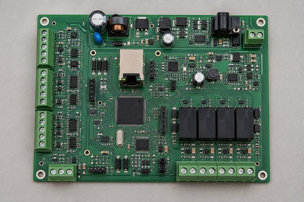
The board uses a closed decision chain. It reads a credential, verifies system conditions, authorizes or denies access, switches the lock and confirms the resulting door state. Breaking that chain into functional blocks makes schematic review, layout and testing easier.
- Processing and memory: An MCU or MPU runs credential, schedule, event and communication logic, while nonvolatile memory protects configuration and logs.
- Reader interfaces: Wiegand inputs, OSDP/RS-485 transceivers or other application-specific interfaces receive credentials and reader status.
- Supervised inputs: Door contacts, request-to-exit, tamper and fire-release inputs report real field conditions and should reject noise and wiring faults.
- Lock outputs: Relays or protected electronic switches control strikes, magnetic locks, bolts and alarm devices.
- Power tree: Input protection, DC/DC conversion, LDO rails, brownout monitoring and optional backup-power supervision keep logic stable during lock transients.
- Network and security: Ethernet, RS-485, CAN or approved wireless modules connect the controller while secure boot, protected keys and authenticated updates limit attack paths.
2-Door vs 4-Door vs Multi-Door Access Control PCB: What Is the Difference?
Door count changes the complete I/O and power architecture. Each added door multiplies reader ports, monitored inputs, lock loads, terminal density, power distribution and test coverage. Architecture should follow wiring topology and failure containment rather than fitting the maximum number of doors onto one PCB.
| Controller type | Typical fit | Design focus | Main trade-off |
| 2-door | Small sites, elevator or cabinet zones | Compact I/O, simple service access | More panels for larger sites |
| 4-door | Commercial floors and distributed entrances | Terminal organization, relay spacing and shared power | Higher wiring and thermal concentration |
| Multi-door | Scalable buildings and campuses | Segmented buses, expansion I/O and fault isolation | Greater firmware, network and validation complexity |
A four-door controller should still allow one faulty reader cable or lock circuit to be isolated without disabling unrelated doors. Multi-door products often benefit from a controller-plus-expansion architecture because shorter field runs, replaceable I/O modules and defined power domains simplify service.
What Are the Main Door Access Control PCB Design Requirements?
Freeze the complete requirements before selecting components. They must cover field wiring, power behavior, security, environmental limits and testability. Starting with an MCU and adding interfaces later usually creates grounding, connector and firmware constraints.
- I/O matrix: Define every reader, lock, contact, exit input, alarm, tamper signal and expansion port, including inactive and fault states.
- Power budget: Separate controller consumption from reader and lock loads, then evaluate startup, release, simultaneous-door and backup-power cases.
- Safety behavior: Document fail-safe or fail-secure operation, fire-release interaction, manual egress and required behavior after processor or communication failure.
- Cybersecurity boundary: Identify trusted devices, exposed ports, credential storage, service access, update paths and key provisioning.
- Mechanical definition: Confirm enclosure, mounting holes, terminal direction, cable bend space, indicator visibility and service clearance.
- Verification plan: Provide programming, test points, simulated door fixtures and pass/fail criteria before layout release.
| Required input | Design action | Verification evidence |
| Door and I/O schedule | Map every reader, lock, door contact, exit input, tamper input and alarm channel to its normal, active, open-wire and short-wire state. | Approved I/O matrix and channel-by-channel fixture test. |
| Lock and reader power data | Calculate standby, startup, inrush, single-door, simultaneous-door and backup-supply loads, including cable voltage drop. | Power budget, rail measurements and brownout test record. |
| Reader and network protocols | Define port count, voltage, bit format or device address, baud rate, bus topology, termination and required security mode. | Interface specification and communication test log. |
| Safety and recovery behavior | Define fail-safe/fail-secure operation, emergency release, restart state, offline rules and event recovery. | State-transition matrix with pass/fail acceptance criteria. |
| Enclosure and installation data | Lock board outline, mounting holes, terminal direction, cable bend space, airflow and service access before placement. | Mechanical drawing and enclosure-fit review. |
How Should RFID, Wiegand and OSDP Reader Interface Circuits Be Designed?
Match each reader circuit to its protocol and cable environment. A generic input stage cannot satisfy every electrical and security requirement. RFID describes the credential technology; Wiegand and OSDP describe common reader-to-controller communication paths.
Wiegand inputs require defined logic thresholds, input protection, filtering and a grounding strategy appropriate to cable length and reader supply. Because implementations use different bit formats, firmware should validate format and parity rather than assume every reader is identical. OSDP uses an RS-485 physical layer and supports supervised bidirectional communication. OSDP compatibility alone does not prove that Secure Channel is active; configuration and bench testing must verify the required security mode.
- Protect the connector first: Place ESD and transient components close to the reader terminal before traces enter the logic area.
- Control the RS-485 bus: Plan termination, biasing, topology, common-mode range and reference conductor from the complete cable installation.
- Separate power noise: Do not route reader data alongside relay contacts, lock-current loops or switching-node copper.
- Support service diagnosis: Expose protocol, supply and ground test points without creating an unsecured debug path.
| Decision point | Wiegand | OSDP |
| Communication | Simple one-way data signaling with implementation-specific credential formats. | Addressed, bidirectional communication over an RS-485 physical layer. |
| Monitoring | Limited interface supervision; wiring faults may need separate detection. | Supports supervised communication and reader status reporting. |
| Security planning | Useful for legacy compatibility, but credential data is not protected by the interface itself. | Secure Channel can protect reader-panel traffic when correctly configured and verified. |
| Best fit | Existing readers, controlled migration and products that must retain legacy support. | New designs that need interoperability, diagnostics, multidrop capability and stronger communication security. |
How Should the Door Lock Control Circuit, Relay Output and Power Supply Be Designed?
Size the lock-control stage from the real load profile. Include steady-state current, inrush, release behavior and the fail-safe requirement, not only the nameplate voltage. Relay contacts can provide useful isolation, while MOSFET outputs can add diagnostics and fast protection.
- Confirm the load: Record lock type, nominal voltage, steady current, inrush, release time and fail-safe or fail-secure behavior.
- Select the output: Use dry relay contacts when isolation and polarity flexibility are required; consider protected MOSFET outputs when diagnostics, switching speed or electronic current limiting are needed.
- Control inductive energy: Match the flyback diode, TVS or clamp network to the load and required release time. A simple diode lowers voltage stress but can slow release.
- Protect each channel: Coordinate contact rating, conductor width, terminal rating, fuse or resettable protection and short-circuit recovery.
- Protect the logic rail: Include cable voltage drop and simultaneous lock events in the power budget so a door command cannot reset the processor or corrupt event memory.
Power sequencing should define startup, battery switchover, brownout and restart behavior. The design review must also state whether an emergency input removes lock power in hardware, firmware or both, according to the system requirements and local regulations. Verification should record rail voltage, processor reset status, relay state and event-memory integrity during each transition.
How to Protect a Door Access Control Board from ESD, Surge and Wiring Faults?
Use layered protection at every field port. Limit energy at the connector, control current, prevent reverse paths and keep residual transients away from logic. One TVS diode added late in layout is not a complete protection plan.
- ESD path: Use short, low-inductance connections from the protective device to the intended reference or chassis path.
- Surge coordination: Select TVS, series impedance, fusing and downstream ratings so each layer survives the expected waveform.
- Miswiring tolerance: Evaluate reverse polarity, reader power shorts, lock-output shorts, cross-connected terminals and hot-plug events.
- Galvanic and ground strategy: Decide where isolation is necessary and avoid accidental return paths through communication shields or mounting hardware.
- Recovery behavior: Verify that a protected fault clears safely and does not leave a relay, processor or communication port in an undefined state.
How Should a Networked Access Control Board Be Designed for Secure Communication?
Secure communication begins with a protected device identity. It also requires authenticated sessions, controlled updates and safe local operation when the network is unavailable. Adding Ethernet or Wi-Fi without defining trust boundaries increases the attack surface.
- Protect device identity: Provision a unique device identity and keep long-term keys in a protected device or secure region.
- Authenticate code and updates: Verify firmware before execution, accept updates only from authorized sources and prevent an interrupted or failed update from leaving an unusable controller.
- Reduce exposed interfaces: Disable unnecessary production debug access, limit services and separate installer, administrator and application permissions.
- Use standard security protocols: Authenticate management sessions, protect data in transit, rate-limit repeated attempts and record security-relevant events.
- Define offline operation: Specify which cached users and schedules remain valid, how clock integrity is maintained, how many events can be stored and how records are synchronized after reconnection.
What PCB Materials, Stackups and Layout Rules Are Suitable for Access Control Boards?
Choose material and stackup from the application requirements. Most controllers can use a suitable FR-4 construction, but layer count and material grade should follow routing density, EMC, operating temperature and reliability needs. Confirm the construction against the actual product specification.
A four-layer stackup often gives a continuous ground reference and cleaner power distribution than a crowded two-layer board. Keep the network magnetics or transceiver region, processor, reader interfaces, switching regulators and relay contacts in clear functional zones. Do not split the return path beneath high-speed or noise-sensitive traces. Provide creepage and clearance appropriate to the actual working voltage, pollution environment and governing safety requirements.
- Field terminals: Place protection and filtering beside the connector and label channels consistently.
- Relays and lock power: Separate contact copper from low-voltage logic and control heat around high-current connections.
- Ethernet or RF: Follow the transceiver/module reference layout, impedance and keep-out requirements.
- Manufacturing access: Provide fiducials, programming pads, test points and realistic probe clearance.
| Stackup choice | Suitable use | Release check |
| Two layers | Lower-density controllers with modest interface speed and enough area for uninterrupted return paths. | Confirm grounding, relay-current routing, thermal paths and EMC margin on the finished layout. |
| Four layers | Networked or denser boards that benefit from a continuous ground plane and more controlled power distribution. | Approve the stackup, reference planes, impedance needs, via structure and fabrication availability before routing. |
| More than four layers | Use only when routing density, memory buses, RF, isolation or mechanical constraints justify the added process complexity. | Document the electrical reason for each added layer and verify manufacturability with the selected supplier. |
How Are Door Access Control PCBs Manufactured and Assembled?
Use a controlled release-to-acceptance sequence. Manufacturing should progress from engineering-data review through fabrication, assembly, programming and functional acceptance. Terminal blocks, relays, tall capacitors and network connectors make process planning as important as the SMT stage.
- Engineering data and DFM review: Check Gerber or ODB++, NC drill, stackup, fabrication drawing, BOM, centroid data, polarity, assembly drawings, firmware and test instructions; issue one consolidated question list before release.
- Bare PCB fabrication: Build the approved stackup, image and etch copper, drill and plate holes, apply solder mask and finish, route the profile, then complete electrical test and dimensional inspection.
- Incoming component verification: Confirm relay contact ratings, protection-device identity, connector pitch, polarized parts, moisture sensitivity and approved substitutions against the released BOM.
- Solder-paste printing and SPI: Verify paste volume and alignment before placement, with stencil apertures reviewed for fine-pitch and thermal-pad components.
- SMT placement and reflow: Place components using the approved centroid and polarity data, then control the reflow profile for the actual component and board mix.
- Through-hole assembly: Install relays, terminal blocks and other tall or high-current parts using the defined selective-solder, wave-solder or controlled hand-solder process.
- Inspection: Use AOI for visible SMT joints and polarity; apply risk-based X-ray to hidden or bottom-terminated joints when the package and acceptance plan require it.
- Programming and functional acceptance: Load the approved firmware, provision required unit data and run the reader, input, relay, network, power-transition and fault tests before release.
EBest Circuit’s service scope covers PCB design, production and assembly, including prototype builds and component sourcing. Available material and product experience includes FR-4, multilayer, high-Tg, high-speed and impedance-control PCB families; the final construction and process remain subject to project review.
What Testing Is Required for a Door Access Control PCB Assembly?
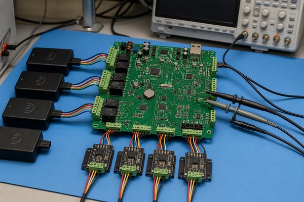
Test every channel and critical state transition. A processor boot test alone is insufficient. A production fixture should simulate readers, door contacts, exit inputs, lock loads, network traffic, power interruption and fault conditions with recorded pass/fail limits.
- Bare-board checks: Electrical test and fabrication inspection confirm continuity, isolation, dimensions and specified construction.
- Assembly inspection: SPI, AOI and risk-based X-ray identify paste, placement and solder-joint defects.
- Programming and identity: Load approved firmware, protect production interfaces and record the required unit identifiers.
- I/O functional test: Exercise all readers, supervised inputs, relays, indicators, buzzers and expansion channels.
- Power and fault test: Check startup, brownout, backup transition, shorted field ports, reversed input and simultaneous lock events as specified.
- Communication test: Verify Ethernet/serial links, OSDP behavior, reconnect logic and the required secure session functions.
A repeatable production test needs more than a technician’s visual judgment. The released fixture package should identify connector pinout, simulated loads, firmware version, measurement points, numerical limits, expected relay and indicator states, failure codes and the records retained for each unit. A known-good reference assembly helps confirm that fixture maintenance has not changed the test result.
What Custom Door Access Control PCB Manufacturing and Assembly Services Can We Provide?
Define custom support through measurable deliverables. It can cover design files, prototype risk reduction, sourced components, assembled controllers and repeatable production data. This is more useful than a vague turnkey promise.
- Design support: Schematic and layout review for reader interfaces, lock outputs, power integrity, protection, stackup and test access reduces avoidable respins.
- Prototype build: A controlled sample build exposes connector, programming, firmware and fixture issues before volume tooling is fixed.
- Component sourcing: BOM review and approved substitution control protect electrical ratings and firmware compatibility.
- Fabrication and assembly: One coordinated data package reduces responsibility gaps between bare-board and PCBA suppliers.
- Fast-delivery review: EBest Circuit offers expedited service, including urgent bare-board shipment within 24 hours when the material, complexity, quantity and production data make that schedule feasible.
- Quality evidence: EBest Circuit lists ISO 9001:2015, ISO 13485:2016, IATF 16949, AS9100D, UL, RoHS and REACH; each order should identify which certification scope, inspection records and acceptance criteria are relevant.
To shorten engineering review and quotation time, submit one controlled package containing the current PCB data, BOM, quantities, reader and lock specifications, enclosure drawing, firmware responsibility, programming method and acceptance test. Clearly mark unresolved items and approved alternatives so they can be closed before material purchasing begins.
4-Door Networked Access Control PCB Manufacturing and Assembly Case Study
A credible case needs a traceable evidence chain. This representative project shows how an incomplete four-door controller package can become a controlled build release without claiming an unverified customer identity, yield, delivery result or field-performance figure.
Project Background: A security-equipment team required one board to manage four doors, exchange events with network software and retain defined local operation during a server interruption. The hardware included four reader channels, monitored door and exit inputs, four lock outputs, Ethernet, nonvolatile event memory and a protected DC input.
Project Requirements: The team supplied Gerber/ODB++, NC drill, stackup, BOM, centroid data, assembly drawings, firmware and an initial functional-test description. Before release, the requirements matrix still needed confirmed lock voltage and inrush, Wiegand/OSDP allocation, RS-485 termination, emergency-release logic, offline user and event limits, enclosure clearances and production-key handling.
Our Solution: Engineering converted those open items into one tracked question list and held fabrication until the electrical and mechanical answers were approved. The layout review separated reader, Ethernet, logic, regulator and relay-current zones; checked current paths, terminal ratings and protection placement; and aligned programming and measurement pads with the fixture. The process plan then defined SMT, through-hole relay and terminal assembly, AOI, risk-based X-ray, controlled provisioning and four-channel functional testing.
Output Results: The release package contained the approved design revision, resolved engineering-question log, controlled BOM, fabrication and assembly data, programming instructions, fixture connection map and pass/fail test definition. Fabricated boards and assembled units could therefore be checked against the same revision and acceptance criteria, while the retained package established a traceable baseline for repeat orders.
Why Choose EBest Circuit as Your Door Access Control PCB Manufacturer?
Choose a partner that closes responsibility gaps. Access-control requirements must become reviewable files, controlled parts, testable assemblies and clear responsibility boundaries. Company history or certificate names alone do not prevent a door-controller failure.
- One engineering path: Coordinating design, fabrication, sourcing and assembly reduces handoff gaps when a reader, relay, connector or firmware requirement changes.
- Prototype-to-production continuity: Keeping approved files, substitutions and test requirements together reduces the chance that a corrected sample issue returns in volume builds.
- Application-matched construction: Access to FR-4, multilayer, high-Tg, high-speed and impedance-control PCB options supports selection based on the actual network, thermal and mechanical requirements.
- Order-specific quality planning: Listed management-system and product-compliance credentials can support supplier qualification, while each order still defines its own inspection, traceability and acceptance evidence.
- Feasible expedited planning: Early material and process review turns a general fast-delivery request into a schedule that identifies the real start condition and remaining risks.
EBest Circuit can review the controller architecture and manufacturing package before quotation, helping the project team identify missing power, interface, test and sourcing details early.
FAQs About Door Access Control PCBs
These questions cover procurement and implementation details that are useful but do not repeat the main design sections.
Q1: What files are needed to quote a door access control PCB assembly?
A1: Submit Gerber or ODB++, NC drill, BOM, centroid data and assembly drawings first. Add the stackup, firmware, programming method, test procedure, quantities and approved-substitution rules so fabrication and PCBA scope can be reviewed together.
Q2: How should event logs be protected during sudden power loss?
A2: Use power-fail detection, bounded write operations and a storage method that tolerates interrupted updates. Testing should remove input power at different points in an event write, then confirm that existing records, the newest valid record, indexes and the restart state remain consistent.
Q3: What environmental tests are useful for an access control controller?
A3: Select tests from the declared installation environment and product requirements. Useful checks may include operating-temperature cycling, humidity exposure, powered thermal testing, vibration where relevant and repeated connector or relay operation. Test limits and acceptance criteria must come from the actual product specification.
Q4: How should the real-time clock and time synchronization be validated?
A4: Verify time accuracy, backup retention, timezone handling and recovery after network and power interruptions. The test plan should also check daylight-saving behavior where applicable, server resynchronization and the order of event records created before and after a clock correction.
Q5: How should a tamper input be handled?
A5: Treat tamper as a supervised security input with a defined normal, alarm and wiring-fault state. Its circuit, polling and event handling should match the enclosure and system threat model.
Q6: Is conformal coating required for access control boards?
A6: Coating is application-dependent, not an automatic requirement. Review humidity, condensation, contamination, connector masking, repairability and coating compatibility, then specify the material and inspection criteria if needed.
Q7: Can relays be replaced by MOSFET outputs?
A7: Sometimes, but the electrical behavior and isolation are different. Compare polarity, load type, leakage, diagnostic needs, transient energy, fail-state behavior and service expectations before changing the output topology.
Q8: How are unique device credentials programmed during production?
A8: Use a controlled provisioning process that writes and verifies unit-specific data without exposing reusable secrets. The factory test plan should define access control, logging, reject handling and debug-port closure.
Q9: What causes intermittent reader communication after installation?
A9: Common causes include wiring topology, grounding, termination, voltage drop, noise coupling and protocol configuration. Capture cable length, reader type, power at the reader and communication errors before blaming firmware or the PCB.
Q10: How should component substitutions be controlled for a repeat order?
A10: Maintain an approved BOM and require technical review before any substitute is released. Relays, TVS devices, transceivers, memory and connectors can alter ratings, firmware behavior or mechanical fit even when packages appear compatible.
Conclusion
A reliable door access control PCB starts with a complete I/O, power, security and failure-behavior definition. Reader interfaces, lock loads, field protection, network security, PCB layout and production tests must then be verified as one control chain.
An early engineering review can expose reader-interface, lock-power, protection, enclosure and test-fixture risks before they become prototype respins or production delays. EBest Circuit can coordinate design review, PCB fabrication, component sourcing, assembly, programming preparation and order-specific testing through one controlled project package.
For custom door access control PCB design, prototyping, fabrication, component sourcing and assembly, send your Gerber/ODB++, NC drill, stackup, BOM, centroid data, firmware, quantities and test requirements to sales@bestpcbs.com for engineering review and a quotation.
You may also like





Tags: Access Control Board, Access Control PCB Assembly, Door Access Control PCB, Door Controller PCB