





A 2 layer PCB is usually the right choice for simple, low-speed, low-density circuits where bare-board cost matters most. A 4 layer PCB is usually the better choice when the design needs cleaner return paths, better EMI control, easier routing, stronger power distribution, or more reliable high-speed behavior.
The practical decision is not only “two layers are cheaper” or “four layers are better.” The best layer count depends on circuit density, signal edge speed, power integrity, board size, EMC risk, connector placement, assembly yield, and the cost of redesign if the first prototype fails.
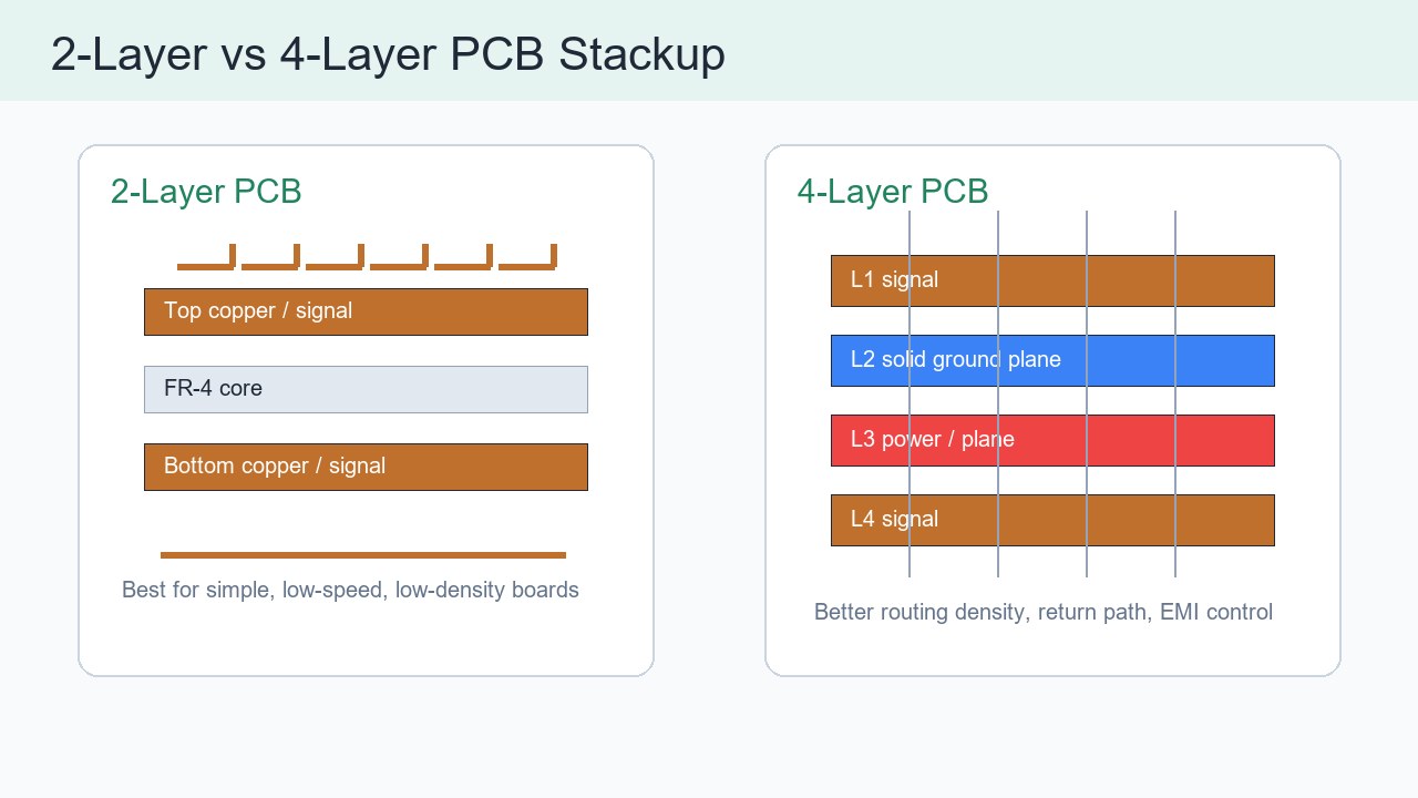
Quick Answer: Choose 2 Layer for Simplicity, 4 Layer for Performance Margin
Choose a 2 layer PCB when the circuit is simple enough to route cleanly without cutting the ground path. Choose a 4 layer PCB when the board needs continuous reference planes, dense routing, lower loop area, or better control of EMI and signal integrity.
| Decision Factor | 2 Layer PCB | 4 Layer PCB | Engineering Note |
| Best fit | Simple control boards, LED boards, basic power boards, low-speed sensors | MCU boards, wireless products, mixed-signal boards, compact electronics | Layer count should follow routing and noise risk, not habit. |
| Routing density | Limited to top and bottom copper | Outer routing plus inner reference and power planes | 4 layers often reduce routing compromises. |
| EMI control | Depends heavily on layout discipline and ground pours | Easier to maintain short return paths with a solid plane | Continuous reference planes reduce loop area. |
| Cost | Lower bare-board cost | Higher bare-board cost, sometimes lower debug cost | For dense designs, 4 layers may save engineering time. |
| Manufacturing risk | Easy to inspect and fabricate | Needs stackup control, lamination, and clearer documentation | Ask for stackup, impedance, and inspection requirements early. |
What Is a 2 Layer PCB?
A 2 layer PCB has copper on the top and bottom sides of the board, separated by an insulating core. It can route signals on both sides, use vias to change layers, and use copper pours for ground or power distribution.
Two-layer boards are common in basic industrial controls, small LED products, simple power distribution, connector adapters, low-speed sensor boards, and cost-sensitive prototypes. The main limitation is that every trace, via, connector, and copper pour competes for the same two copper layers.
What Is a 4 Layer PCB?
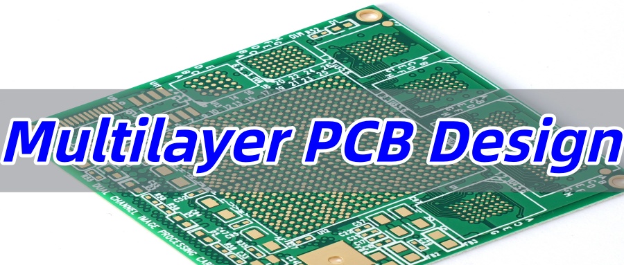
A 4 layer PCB has four copper layers separated by dielectric material. A common structure is top signal, inner ground plane, inner power plane, and bottom signal, although the best stackup should be confirmed with the PCB manufacturer and the design requirements.
The main advantage is not only “more routing layers.” A 4 layer PCB can place signal traces close to a continuous reference plane, which gives return current a predictable path and helps reduce radiation, crosstalk, and ground bounce. This is why many compact digital products start at four layers even when the schematic looks moderate.
2 Layer vs 4 Layer PCB Stackup Differences
The biggest stackup difference is that a 4 layer board can dedicate inner copper to planes, while a 2 layer board must share copper for signals, power, and ground. That changes the way current returns, how decoupling capacitors behave, and how easily the layout can pass EMC testing.
| Stackup Item | 2 Layer PCB | 4 Layer PCB | Buyer or Engineering Note |
| Typical layers | Top copper and bottom copper | Top signal, ground plane, power or plane layer, bottom signal | Actual construction varies by supplier and thickness. |
| Reference plane | Ground pour may be interrupted by routing | Solid inner ground plane is practical | Ask whether critical signals cross plane splits or voids. |
| Power distribution | Wider traces or pours are needed | Power plane or large inner copper can reduce impedance | High-current boards still need thermal and copper-width checks. |
| Impedance control | Harder and less predictable | More practical with controlled dielectric and planes | Request impedance coupon and stackup data when required. |
| Board thickness | Often simple standard thickness | Needs defined dielectric and copper arrangement | Confirm finished thickness, copper weight, and tolerance. |
When a 2 Layer PCB Is the Better Choice
A 2 layer PCB is better when the circuit can be routed with clean grounding, enough spacing, and no high-speed or EMI-critical constraints. It is also attractive when the product needs a simple bare board, a low prototype cost, or very easy visual inspection.
- The board has low-speed digital signals, simple analog paths, or basic switching.
- The board size is not tightly constrained, so wider traces and ground pours fit.
- The product is cost-sensitive and does not need controlled impedance.
- The design has low component density and no fine-pitch BGA or dense connector field.
- The EMC environment is mild and the enclosure, cable, and power system are simple.
A good 2 layer design still needs disciplined grounding. Avoid narrow ground traces, long return loops, poor decoupling placement, and random copper islands that look like ground but do not provide a reliable return path.
When a 4 Layer PCB Is the Better Choice
A 4 layer PCB is better when the board needs routing freedom and electrical margin. The additional layers help the designer maintain a continuous reference plane, route around dense components, and separate power distribution from sensitive signal paths.
- The board includes fast digital edges, USB, Ethernet, RF modules, DDR, high-speed ADCs, or dense MCU routing.
- Ground return paths are broken or difficult to control on a 2 layer layout.
- The product must reduce EMI risk before compliance testing.
- The PCB must be compact, connector-heavy, or packed with fine-pitch components.
- The design needs a stable power distribution network and better decoupling behavior.
For many commercial products, 4 layers are used because the extra bare-board cost is smaller than the risk of a failed EMC test, unstable prototype, or repeated layout cycle.
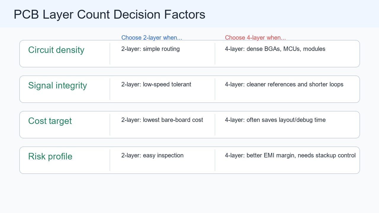
Cost Difference: Bare Board Price vs Total Project Cost
A 2 layer PCB usually has the lower bare-board price, but a 4 layer PCB can lower total project cost when it prevents redesign, noise troubleshooting, or EMC failure. Procurement should compare the full cost of the design decision, not only the first PCB quotation.
| Cost Area | 2 Layer PCB Impact | 4 Layer PCB Impact | What to Check Before Ordering |
| Bare PCB fabrication | Usually lower | Usually higher due to lamination and extra copper layers | Compare quantity, size, copper weight, finish, and delivery time. |
| Layout time | Can increase if routing is congested | Often easier for dense boards | Ask whether the designer is forcing a 2 layer board too far. |
| EMI debugging | Higher risk on noisy or cable-connected products | Lower risk when planes and decoupling are designed well | Consider EMC test cost and project schedule impact. |
| Assembly yield | Good for simple boards | Good when routing supports clean placement and test access | Check test points, panelization, and soldering access. |
| Future revisions | May need a layer-count upgrade later | More margin for product updates | Consider whether the product roadmap adds functions. |
Signal Integrity and EMI: Why Ground Planes Matter
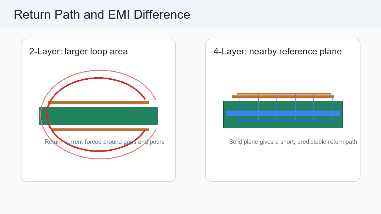
Signal integrity and EMI are often the reason a design moves from 2 layers to 4 layers. A solid ground plane under signal traces gives return current a short path, reduces loop area, and helps contain electromagnetic fields.
On a 2 layer board, ground pours can help, but they are frequently cut by routing channels, vias, slots, connectors, and power traces. When the return path has to detour, the loop area grows. Larger loops are more likely to radiate noise and pick up noise from nearby switching circuits.
Routing Density and Component Placement
A 4 layer PCB makes routing easier when components are dense, but it does not replace good placement. Put connectors, power sections, clocks, high-current paths, and sensitive analog areas in logical zones before deciding whether two layers are enough.
For a 2 layer design, routing congestion often causes long traces, extra vias, narrow ground necks, and poor test-point access. For a 4 layer design, routing can be cleaner, but the designer must still avoid plane splits under critical signals and document which layers are used for reference and power.
Manufacturing and Quality Control Differences
A 2 layer PCB is simpler to fabricate, while a 4 layer PCB needs tighter control of lamination, registration, dielectric thickness, and stackup documentation. This does not make 4 layer boards risky, but it does mean the supplier should receive clearer fabrication notes.
- Confirm finished thickness, copper weight, solder mask, surface finish, and impedance requirements.
- For 4 layer boards, request the stackup before fabrication if impedance, EMI, or mechanical thickness matters.
- Use IPC-A-600 and IPC-6012 acceptance class requirements when they are part of the buyer’s quality specification.
- Check annular ring, drill tolerance, minimum trace/space, solder mask bridge, and via fill or tenting requirements.
- Keep test points accessible, especially when the 4 layer design is dense and assembled with fine-pitch parts.
Common Mistakes When Choosing Layer Count
The most common mistake is choosing the layer count by price alone. Another common mistake is assuming that a 4 layer PCB automatically fixes EMI, even when the stackup has poor reference planes or signals cross plane gaps.
| Mistake | Why It Matters | Better Decision |
| Forcing dense routing onto 2 layers | Creates long traces, broken ground paths, and hard-to-debug noise | Compare 4 layer cost against redesign and EMC risk. |
| Using 4 layers without a clear stackup | Planes may not support the signals that need them | Define layer order, reference plane, and dielectric targets. |
| Ignoring power return paths | High-current loops can heat copper and radiate noise | Review power width, copper weight, via count, and thermal path. |
| Comparing quotes with different specs | Price differences may come from finish, copper, test, or delivery | Use the same Gerber, stackup, quantity, finish, and test requirements. |
| Skipping DFM review | Small layout problems can become production defects | Ask the PCB supplier for DFM feedback before mass production. |
Procurement Checklist Before Ordering 2 Layer or 4 Layer PCB
Procurement should ask technical questions before comparing price, because layer count affects quality requirements, lead time, and manufacturing control. A clear RFQ reduces quotation errors and avoids surprise engineering changes.
- What is the finished board thickness and tolerance?
- What copper weight is required on outer and inner layers?
- Does the design require controlled impedance or impedance testing?
- What minimum trace/space, drill size, annular ring, and solder mask bridge are used?
- Is electrical test required for every board?
- Are there high-current, RF, high-speed, or mixed-signal areas that need engineering review?
- Does the supplier provide DFM feedback before production?
- For 4 layer PCB, can the supplier confirm the proposed stackup before fabrication?
Best Practical Selection Rule
The best rule is to use 2 layers only when the board remains electrically clean, manufacturable, and easy to test. Use 4 layers when the design needs a controlled reference plane, better routing density, or more performance margin than a 2 layer layout can provide.
For early prototypes, a 2 layer board may be enough to validate a simple circuit. For products with cables, switching power, fast digital interfaces, dense modules, or EMC exposure, starting with 4 layers often produces a cleaner design path.
FAQ About 4 Layer vs 2 Layer PCB
Is a 4 layer PCB always better than a 2 layer PCB?
No. A 4 layer PCB is usually better for dense routing, EMI control, and signal integrity, but a 2 layer PCB can be the better choice for simple, low-speed, cost-sensitive designs.
When should I upgrade from 2 layer to 4 layer PCB?
Upgrade when routing is congested, return paths are broken, EMI risk is high, impedance control is needed, or the board includes dense ICs, fast edges, wireless modules, or mixed-signal sections.
Is a 4 layer PCB much more expensive?
It is usually more expensive as a bare PCB because it needs more copper layers and lamination. However, the total project cost can be lower if 4 layers reduce redesign, EMI debugging, or layout time.
Can a 2 layer PCB pass EMI testing?
Yes, many 2 layer boards can pass EMI testing when the layout, grounding, filtering, enclosure, and cable design are well controlled. The risk rises when the board has fast edges, switching power, long cables, or broken return paths.
What is the common 4 layer PCB stackup?
A common stackup is signal, ground plane, power plane, and signal. Some designs use two ground reference layers or different plane arrangements. The right stackup should be confirmed with the manufacturer and the design requirements.
Is a 2 layer PCB suitable for LED products?
Often yes. Simple LED boards can use 2 layers when current, heat, copper width, and voltage drop are controlled. High-power LED boards may need heavier copper, metal-core PCB, or special thermal design instead of simply adding layers.
Does a 4 layer PCB improve heat dissipation?
It can help spread heat when inner copper planes are designed as part of the thermal path, but layer count alone is not a thermal solution. Copper weight, via arrays, board material, component placement, and enclosure contact matter more.
Can I route high-speed signals on a 2 layer PCB?
Some moderate-speed designs can work on 2 layers, but high-speed signals become harder to control because the return path and impedance are less predictable. For reliable high-speed interfaces, 4 layers are usually a safer starting point.
Do I need controlled impedance for every 4 layer PCB?
No. Controlled impedance is needed when the interface or signal speed requires it. If needed, specify impedance values, tolerance, layer reference, stackup, and test requirements in the fabrication notes.
Which is better for prototypes, 2 layer or 4 layer PCB?
Use 2 layers for simple proof-of-concept prototypes where cost and speed matter. Use 4 layers when the prototype must represent real EMI, signal integrity, power integrity, and product-size constraints.
Can a 4 layer PCB make assembly harder?
Layer count itself does not usually make assembly harder, but dense 4 layer layouts may reduce test access and increase placement complexity. Keep test points, fiducials, panelization, and soldering clearance in the DFM review.
What should I send to a supplier for a 4 layer PCB quote?
Send Gerber files, drill files, BOM if assembly is required, stackup requirements, finished thickness, copper weight, surface finish, impedance requirements, solder mask color, quantity, test requirements, and delivery expectations.
Final Recommendation
For a simple low-speed board, 2 layers can be the most economical and practical choice. For dense electronics, high-speed interfaces, EMI-sensitive products, compact layouts, or production designs where failure is expensive, 4 layers usually provide better engineering margin.
If you’re sourcing reliable PCB/PCBA manufacturing, including OEM, ODM, prototyping, mass production, or custom engineering solutions, reach out to our engineering team for technical support and a quote at sales@bestpcbs.com.
You may also like



Tags: 2 layer PCB, 4 layer pcb, Multilayer PCB Design, pcb stackup