

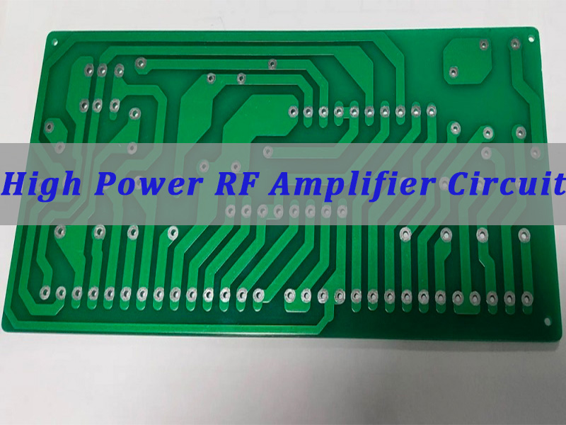
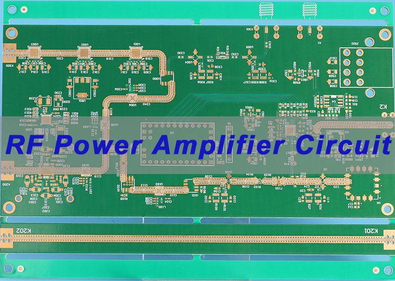
High Power RF Amplifier Circuit is the critical, final-stage components that transform low-power radio frequency signals into powerful, broadcast-ready waves, forming the backbone of modern wireless communication, radar, and industrial systems. This comprehensive guide delves into the intricacies of RF high power amplifier circuit design, exploring its working principles, key components like GaN and LDMOS transistors, the critical role of impedance matching, material selection (including advanced PCB substrates), and its wide-ranging applications, all through the lens of precision manufacturing enabled by a Digital MES Smart Factory.
What are the most common pain points engineers face when moving from high power RF amplifier circuit design to mass production?
- Thermal Runaway: Poor heat dissipation causes performance drift and device failure.
- Impedance Mismatch: Improper board matching leads to signal reflection and lower RF efficiency.
- Parasitic Oscillations: High-frequency resonances cause instability and unwanted emissions.
- Material Inconsistency: PCB laminate Dk variation disrupts RF performance stability.
- Manufacturing Bottlenecks: Slow prototyping and low visibility delay production schedules.
EBest Circuit (Best Technology) provides the following solutions.
- Advanced Thermal Management: Optimized thermal design with vias and metal-core or ceramic substrates.
- Impedance-Controlled Fabrication: Precise simulation and manufacturing ensure stable impedance.
- Stability-Focused PCB Layout: Layout minimizes parasitic effects and prevents oscillation.
- High-Frequency Material Selection: Supports FR-4, Rogers, and other low-loss RF materials.
- Digital MES Smart Manufacturing: Real-time production tracking and faster prototyping cycles.
EBest Circuit (Best Technology) specializes in high-frequency and high-reliability PCB and PCBA manufacturing. Our expertise is uniquely amplified by our Digital MES Smart Factory, which provides unparalleled traceability, process consistency, and agility from prototyping to volume production. We bridge the gap between complex RF design and manufacturable reality. For your next project, pls feel free to contact our engineering sales team at sales@bestpcbs.com.
What Is A High Power RF Amplifier Circuit And How Does It Work?
A High Power RF Amplifier Circuit is an electronic assembly designed to significantly increase the power level of a Radio Frequency (RF) input signal while maintaining its signal integrity (minimizing distortion). It acts as the final powerhouse in a transmitter chain, converting DC power from a supply into amplified RF energy suitable for radiation through an antenna.
The core operation revolves around an active semiconductor device (transistor) operating in its nonlinear region. Here’s a breakdown of the working principle:
- RF Input Stage: A low-power RF signal is fed into the amplifier’s input port.
- Biasing Network: A DC bias circuit sets the transistor’s operating point (e.g., Class A, AB, B, C) which determines the trade-off between linearity and efficiency.
- Power Amplification: The input RF signal modulates the DC current flowing through the transistor. The transistor, acting as a controlled current source, produces a high-current replica of the input signal at its output.
- Impedance Matching Networks: Critical input and output matching networks ensure maximum power transfer from the source to the transistor and from the transistor to the load (antenna). They also transform impedances for optimal transistor performance.
- Filtering & Output: Harmonic filters may be used to clean the output signal before it is delivered to the load, ensuring compliance with spectral regulations.
In essence, the circuit’s design meticulously controls the transistor’s behavior to efficiently “pump” energy into the RF signal, making a rf high power amplifier circuit fundamental for any application requiring significant wireless transmission power.
How Is A RF High Power Amplifier Circuit Designed For Stable Output Power?
Achieving stable output power in an RF high power amplifier circuit requires a multi-faceted design strategy that goes beyond simple gain. Stability means consistent performance across frequency, temperature, supply voltage variations, and over time, without unwanted oscillations.
The design process focuses on several key pillars:
- Stability Analysis: Engineers use stability factors (like Rollett’s K-factor) derived from S-parameters to ensure the amplifier is unconditionally stable (will not oscillate) for all source and load impedances. This often involves adding stabilization resistors or networks.
- Load-Pull Characterization: This is critical for power amplifiers. Instead of designing for maximum gain, designers use load-pull contours to find the optimal load impedance that delivers the best compromise of output power, efficiency, and linearity for the specific transistor.
- Robust Biasing: The DC bias network must be designed to prevent low-frequency oscillations and maintain the operating point against temperature drift. Active bias circuits with temperature compensation are often used in high-power applications.
- Thermal Design Integration: Electrical design is inseparable from thermal design. The PCB layout must facilitate efficient heat conduction from the transistor die to the heatsink, using thermal vias, exposed pads, and appropriate substrate materials.
- Advanced Simulation: Modern EDA tools allow for co-simulation of electromagnetic (EM) effects (of the PCB traces and matching networks) with nonlinear transistor models, predicting real-world performance and stability margins before fabrication.
| Design Focus | Goal | Common Technique |
|---|---|---|
| Frequency Stability | Prevent oscillation at any frequency. | Stabilization resistors, RC networks. |
| Thermal Stability | Maintain performance as temperature rises. | Thermal simulation, robust heatsinking. |
| Load Stability | Tolerate antenna impedance variations (VSWR). | Use of isolators or designing for ruggedness. |
Therefore, designing for stability is a proactive process of modeling, simulating, and validating all potential failure modes, ensuring the high power rf amplifier circuit performs reliably under real-world, variable conditions.
What Components Are Commonly Used In A High Power RF Amplifier Circuit?
The performance of a high power rf amplifier circuit is dictated by the careful selection and integration of its core components. Each part plays a specific role in signal integrity, power handling, and efficiency.
- 1. Power Transistor: The heart of the amplifier. Technology choice is paramount:
- GaN (Gallium Nitride): The premier choice for new designs, offering very high power density, efficiency, and operational bandwidth at high frequencies.
- LDMOS (Laterally Diffused Metal Oxide Semiconductor): Dominant in high-power, narrow-to-medium band applications like cellular infrastructure, known for robustness and high gain.
- GaAs (Gallium Arsenide): Common in high-frequency, medium-power applications.
- 2. PCB Substrate / Laminate: The foundation. It must have stable electrical properties and excellent thermal conductivity.
- Rogers RO4000® Series: A industry standard for high-frequency, offering low loss and stable dielectric constant.
- PTFE-based Laminates: Extremely low loss, used in critical aerospace and defense applications.
- Metal-Clad/IMS: For extreme thermal management, where the substrate is a thermally conductive dielectric bonded to an aluminum base.
- Ceramic Substrates (Al₂O₃, AlN): Used in high-reliability and high-power-density modules for their superb thermal and RF properties.
- 3. Passive Components:
- RF Inductors & Capacitors: Used in matching, biasing, and DC blocking networks. Must be high-Q, low ESR, and rated for RF currents.
- Resistors: For biasing, stabilization, and termination. Must be non-inductive and thermally stable.
- Ferrite Beads & Chip Filters: Used for decoupling and suppressing low-frequency or power supply noise.
- 4. Supporting Elements:
- Heat Sink / Thermal Interface Material: Essential for dissipating heat from the transistor package to the environment.
- RF Connectors: (e.g., SMA, N-Type) to interface the amplifier board with external systems. Must be high-quality to minimize loss and VSWR.
- Bias Tee / Regulator: Provides clean, stable DC power to the transistor, often with sequencing and protection features.
Selecting the right combination of these components, tailored to the frequency, bandwidth, and power targets, is the first critical step in realizing a successful amplifier design.
How Does Impedance Matching Affect A High Power RF Amplifier Circuit?
Impedance matching is not merely an optimization step; it is a fundamental requirement for the efficient and predictable operation of a high power rf amplifier circuit. Its primary goal is to maximize the transfer of power from the source to the transistor and from the transistor to the load, while also setting the conditions for the transistor to deliver its designed performance.
The effects of proper and improper impedance matching are profound:
- Maximizes Power Transfer: The maximum power transfer theorem states that maximum power is delivered when the load impedance is the complex conjugate of the source impedance. Matching networks perform this transformation, ensuring the RF power generated by the transistor is delivered to the antenna, not reflected back.
- Optimizes Transistor Performance: A power transistor is designed to deliver specified power, efficiency, and linearity into a specific load impedance (typically 50Ω, but the optimum impedance for the transistor itself is rarely 50Ω). The output matching network transforms the 50Ω system impedance to this optimal load-pull impedance.
- Prevents Signal Reflections & Standing Waves: Mismatch causes a portion of the forward power to be reflected back towards the source. This creates standing waves on the transmission lines, leading to:
- Reduced Output Power: Useful radiated power is decreased.
- Increased VSWR: Voltage Standing Wave Ratio rises, stressing components.
- Gain Ripple & Bandwidth Reduction: Frequency response becomes uneven.
- Device Damage: Reflected power is dissipated as heat in the transistor, potentially causing thermal overload and failure.
- Ensures Stability: A mismatched load can reflect energy back into the transistor at a phase and amplitude that causes it to oscillate, even if it is stable under 50Ω conditions. Good matching, combined with stability networks, prevents this.
In summary, impedance matching directly dictates the efficiency, output power, linearity, bandwidth, and reliability of the amplifier. It is the critical “glue” that allows the high-performance transistor and the rest of the RF system to work in harmony.
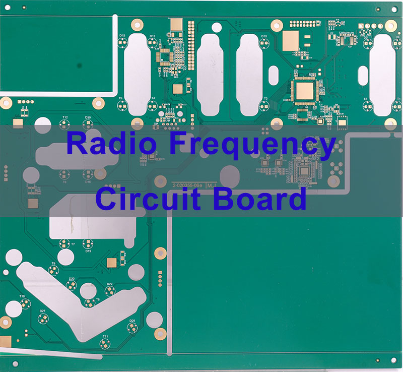
What Materials And PCB Types Are Used For A RF High Power Amplifier Circuit?
The choice of Printed Circuit Board (PCB) material and structure plays a critical role in the performance, cost, and reliability of a rf high power amplifier circuit. Engineers must balance electrical performance, thermal management, manufacturability, and system cost.
At RF and microwave frequencies, PCB materials influence signal loss, impedance stability, and thermal behavior. Selecting the right substrate ensures that the amplifier delivers stable gain, predictable impedance, and reliable long-term operation.
Common PCB Materials Used In RF Power Amplifier Circuits
| Material / PCB Type | Key Properties | Best Use Case in RF PA |
|---|---|---|
| Standard FR-4 | Low cost, higher RF loss | <1 GHz prototypes |
| High-Frequency Laminates (Rogers RO4350B) | Stable Dk, low loss | 2–6 GHz RF amplifiers |
| PTFE Laminates (RT/duroid) | Ultra-low loss | Microwave & mmWave |
| Metal-Clad PCB (IMS) | Excellent thermal dissipation | High-power RF stages |
| Ceramic Substrates (Al₂O₃ / AlN) | High thermal conductivity | Aerospace & microwave |
| LTCC / Thick Film | High integration | Compact RF modules |
This comparison allows engineers to quickly evaluate material suitability before deeper electrical and thermal analysis.
In practice, most commercial high power RF amplifier circuit boards use Rogers high-frequency laminates, because they provide a good balance between RF performance, manufacturing stability, and cost.
PCB Construction Considerations For RF Power Amplifiers
Besides substrate material, the physical PCB structure strongly affects RF performance and thermal stability.
Layer Count
Simple RF amplifiers often use 2-layer boards.
More complex designs typically use 4 or more layers, with dedicated ground planes for shielding and controlled return paths.
Copper Weight
RF power paths often use 2 oz–3 oz copper to:
- Reduce resistive loss
- Improve current capacity
- Enhance thermal spreading
Surface Finish
ENIG (Electroless Nickel Immersion Gold) is widely used because it offers:
- Flat surface for SMT assembly
- Good solderability
- Compatibility with RF components and wire bonding
Why Material Selection Is Critical
Material choice directly influences several critical amplifier parameters:
- RF insertion loss
- impedance stability
- thermal dissipation
- long-term reliability
For this reason, selecting PCB materials is usually one of the earliest engineering decisions when developing a high power RF amplifier circuit. Engineers must evaluate operating frequency, power level, thermal load, reliability requirements, and production cost before finalizing the PCB stack-up.
A well-chosen PCB material ensures that the amplifier performs consistently from prototype validation to full-scale production.
What Are The Main Applications Of A High Power RF Amplifier Circuit?
High Power RF Amplifier Circuits are enabling technologies across a vast spectrum of industries that require the generation of powerful RF signals. Their applications are diverse and critical to modern infrastructure.
- 1. Telecommunications & Cellular Infrastructure: This is the largest market. PAs are the core of every macrocell, small cell, and massive MIMO antenna in 4G/LTE and 5G networks, amplifying signals for user equipment over wide areas.
- 2. Aerospace, Defense & Radar: Used in radar systems for air traffic control, weather monitoring, and military surveillance (ground-based, naval, airborne). They provide the high-power pulses needed for long-range detection and targeting. Also used in electronic warfare (EW) and satellite communications.
- 3. Industrial, Scientific & Medical (ISM):
- Industrial Heating & Plasma Generation: For RF heating, welding, and plasma generation in semiconductor manufacturing (etching, deposition).
- Medical: In Magnetic Resonance Imaging (MRI) systems to generate the RF pulses that excite nuclear spins, and in therapeutic devices for tissue ablation.
- 4. Broadcasting: In FM radio and television transmission towers, high-power PAs broadcast signals over large geographic regions to receivers.
- 5. Research & Scientific Instruments: Used in particle accelerators, plasma physics research, and advanced spectroscopy equipment that require high RF field strengths.
From connecting our smartphones to guiding aircraft and advancing scientific discovery, the rf high power amplifier circuit is a fundamental building block of the wireless world, translating digital information into powerful physical signals that permeate our environment.
Why Should Engineers Choose EBest Circuit (Best Technology) For A RF High Power Amplifier Circuit PCB?
Developing a successful high power rf amplifier circuit requires more than just a PCB fabricator; it demands a manufacturing partner with deep high-frequency expertise and a process built for predictability and speed. Here’s why EBest Circuit (Best Technology) is the ideal partner:
- High-Frequency Specialization: We are not a generic PCB shop. Our engineering team understands the nuances of RF design—impedance control, loss minimization, and layout for stability—ensuring your design intent is faithfully translated into a physical board.
- Material Expertise & Sourcing: We provide expert guidance on material selection, from cost-effective FR-4 hybrids to high-performance Rogers and ceramic substrates. We have reliable supply chains for specialized laminates, preventing project delays.
- Precision, Impedance-Controlled Fabrication: Our manufacturing process is calibrated for high-frequency boards, offering tight tolerances on trace width/spacing (±10% or better on impedance) and precise dielectric thickness control, which is non-negotiable for predictable RF performance.
- Integrated Thermal Management Solutions: We expertly manufacture Metal-Clad PCBs (IMS) and can integrate complex thermal vias and heatsinking recommendations directly into the board design, tackling the primary challenge of high-power RF.
- Speed & Transparency via Digital MES Smart Factory: This is our key differentiator. Our Digital Manufacturing Execution System provides:
- Rapid Prototyping: Streamlined workflows get your prototypes built faster.
- Real-Time Tracking: Monitor your board’s status at every production stage.
- Process Consistency: Automated controls ensure every batch meets the same high standard.
- Data-Driven Insights: Access manufacturing data for continuous improvement of your design.
Choosing EBest Circuit means partnering with a team that speaks the language of RF power amplification, backed by a smart, agile manufacturing system designed to turn complex designs into reliable, high-yield products efficiently.
In summary, high power RF amplifier circuits are the indispensable engines that drive powerful wireless signals, critical to communications, radar, and industrial systems. This article has explored their core principles, design for stability, key components, the vital role of impedance matching, suitable materials, and diverse applications.
Navigating the journey from a schematic to a stable, high-performance amplifier board requires specialized knowledge and manufacturing precision. EBest Circuit (Best Technology) combines deep expertise in high-frequency and thermal management with the agility and transparency of a Digital MES Smart Factory, ensuring your most demanding rf high power amplifier circuit designs are realized with reliability and speed. Pls feel free to contact our team anytime at sales@bestpcbs.com to discuss your RF board project requirements.
FAQs About High Power RF Amplifier Circuit
What Is The Typical Power Range Of A High Power RF Amplifier Circuit?
A high power RF amplifier circuit typically operates from tens of watts to several kilowatts, depending on the application. Communication base stations often use 50–500 W amplifiers, while radar and broadcasting systems may require kilowatt-level RF output power.
What Transistors Are Commonly Used In High Power RF Amplifier Circuits?
Modern high power RF amplifiers commonly use LDMOS, GaN, or GaAs transistors. LDMOS is widely used in cellular infrastructure, while GaN devices are preferred for high-frequency and high-efficiency applications such as radar and satellite communication.
How Do Engineers Prevent Instability In High Power RF Amplifier Circuits?
Engineers improve stability through proper impedance matching, controlled PCB layout, grounding strategies, and stabilization networks. Minimizing parasitic inductance and capacitance is also critical to prevent unwanted oscillations at high frequencies.
Why Is PCB Material Important In A High Power RF Amplifier Circuit?
PCB material affects signal loss, dielectric stability, and thermal management. High-frequency laminates such as Rogers or PTFE-based materials are often used to maintain stable impedance and reduce RF signal attenuation.
You may also like


Tags: High Power RF Amplifier Circuit, RF Amplifier High Power Circuit, rf high power amplifier circuit, rf high power amplifier circuit design