

PCB screen printing is a controlled printing process used in PCB fabrication to apply durable markings and functional coatings—most commonly legend (reference designators, polarity marks, logos) and, in some cases, solder mask patterns—so boards remain readable, traceable, and production-ready.
This article explains how PCB screen printing works in manufacturing, what the PCB screen printing process looks like, how ink and method choices affect quality, and how to choose an experienced partner for PCB and PCBA delivery.
Have you ever received boards where “printing” looked fine at first glance, but later caused assembly confusion, inspection delays, or inconsistent results across batches?
- Unreadable legends that slow down SMT placement checks and manual debug.
- Misaligned markings that cover pads or hide polarity indicators.
- Ink smearing or poor adhesion that flakes after cleaning, handling, or reflow.
- Inconsistent print thickness that creates cosmetic rejects or customer returns.
- Supplier-to-supplier variation where the first lot is acceptable but the second lot looks different.
The best results come from process control, not rework—here are production-grade solutions that map directly to the pain points above:
- Define legend rules (minimum line width, text height, keepout from pads) before release.
- Use registration control and board fiducials to prevent misalignment and pad encroachment.
- Select ink by end-use (chemical resistance, UV cure stability, temperature durability).
- Standardize mesh and squeegee parameters to stabilize print thickness across lots.
- Lock process records and acceptance criteria so repeat orders match the first article.
On the strength of more than 20 years of experience in PCB and PCBA manufacturing, EBest Circuit (Best Technology) delivers stable, production-ready PCB board solutions. Our engineers and customer managers truly know the ropes—they are professionally trained and bring hands-on manufacturing knowledge. Supported by a MES-driven inventory management system, our factories maintain accurate material control, real-time traceability, and predictable delivery performance. We fully recognize that our customers’ trust is invaluable, and we treat every project with the responsibility and transparency. If you need PCB fabrication, SMT assembly, or one-stop PCBA delivery aligned to real manufacturing controls, pls feel free to contact us at sales@bestpcbs.com.
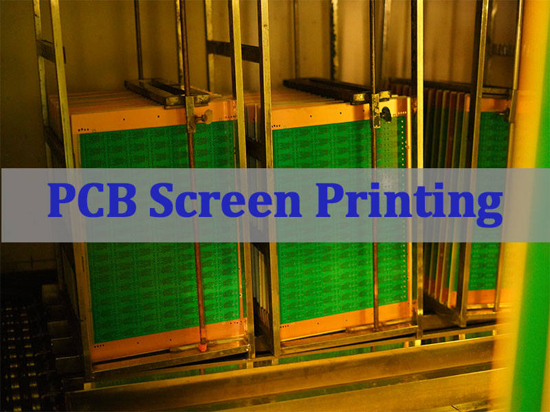
What Is PCB Screen Printing in PCB Fabrication?
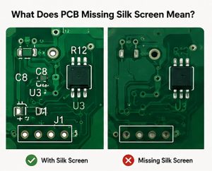
PCB screen printing in PCB fabrication is primarily used to apply silkscreen legends—reference designators, polarity markers, connector IDs, warnings, and logos—so assembly and inspection remain fast and unambiguous. It can also be used for certain mask/ink applications depending on the board type and process route.
Where It Sits in the PCB Flow
In most production lines, PCB screen printing is introduced after core circuit fabrication and before final inspection/pack-out, because the goal is durable identification that survives handling and downstream processing.
What It Commonly Prints
- Reference designators (R/C/U labels)
- Polarity and pin-1 markers
- Test point labels and connector IDs
- Version control codes and date codes
- Customer part numbers and logos
Quick Decision Guide
- If you need high durability markings at volume, screen printing remains a common choice.
- If you need extremely fine graphics or frequent artwork changes, alternate methods may fit better (covered later).
In essence, PCB screen printing is less about decoration and more about production clarity—done right, it reduces human error in assembly and inspection.
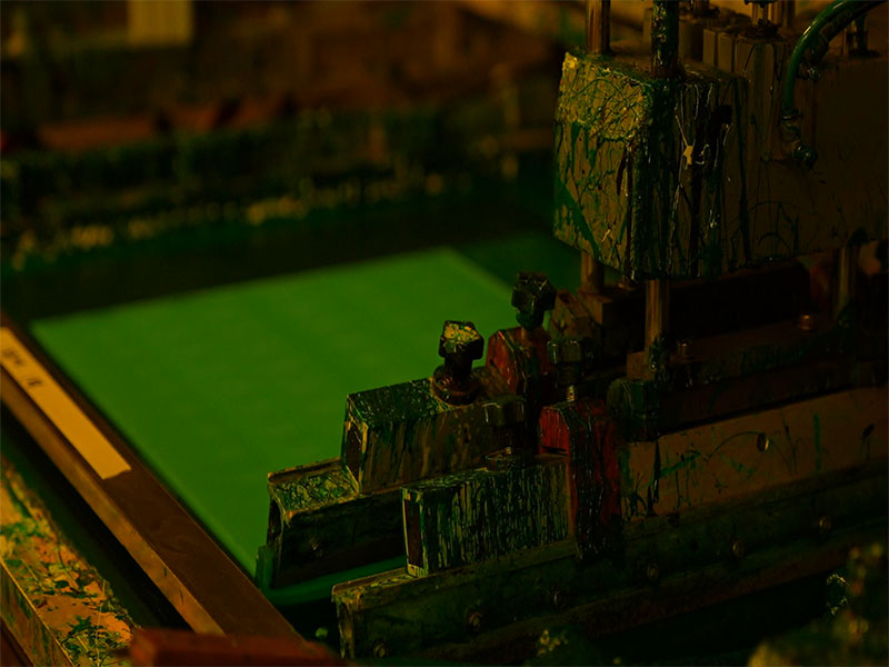
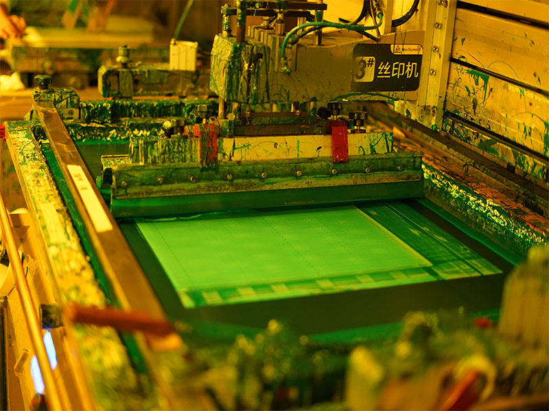
How Does Screen Printing for PCB Work in Manufacturing?
screen printing for PCB works by transferring ink through a patterned mesh onto the board surface using controlled pressure and alignment, then curing the ink to achieve adhesion and abrasion resistance. The manufacturing value is repeatability: the same artwork should print the same way across panels and lots.
What Happens During Printing
- Artwork preparation and screen pattern definition
- Panel alignment using registration features
- Ink transfer via squeegee stroke control
- Curing (UV or thermal) to lock adhesion
- Inspection for clarity, offset, and smear
What Engineers Should Specify
- Minimum text height and stroke width
- Keepout distance from pads and via fields
- Acceptable logo/label placement zones
- Readability targets for AOI and operators
In brief, in manufacturing, screen printing is a controlled transfer + cure system—specification and registration discipline are what make it consistent.
What Is the PCB Screen Printing Process Step by Step?
The PCB screen printing process can be summarized as “align → deposit → cure → verify,” with each step affecting readability and long-term durability. If you want stable results across batches, treat these steps as controlled parameters, not operator preferences.
Step-by-Step Process (Production View)
- Screen Preparation
- Define artwork openings and mesh parameters
- Panel Cleaning
- Remove oils and residues that reduce adhesion
- Alignment and Registration
- Lock placement to prevent offset drift
- Ink Deposition
- Control stroke speed, angle, and pressure
- Curing
- UV/thermal cure to stabilize surface hardness
- Inspection and Lot Records
- Verify readability and adhesion; record settings
Typical Control Points (Concise)
- Registration tolerance
- Mesh selection and tension stability
- Ink viscosity control window
- Cure energy/time window
- Post-cure adhesion check criteria
To sum up, the process is simple to describe but sensitive in execution—repeatability comes from locking parameters and acceptance criteria.
Why Is Silk Screen Printing in PCB Still Widely Used Today?
silk screen printing in PCB remains widely used because it delivers a strong cost-to-durability ratio for high-volume marking needs. It also integrates well into existing PCB production lines, making it practical for both prototypes and mass production when artwork is stable.
Why Manufacturers Keep Using It
- Durable legends for handling and service life
- Efficient for panelized production
- Cost-effective for repeated builds
- Compatible with common PCB finishes and coatings
- Easy to verify visually during assembly
Where It Performs Best
- Industrial boards with stable revision cycles
- Consumer products requiring clear compliance labeling
- Projects with high operator interaction (manual debug/rework)
In summary, screen printing remains popular because it’s scalable, rugged, and production-friendly when legend rules are well defined.
What Screen Printing Method PCB Fabrication Commonly Uses?
The screen printing method PCB fabrication commonly uses depends on the printed layer (legend vs mask), required durability, and the resolution needed. In practice, most lines use optimized mesh + controlled cure systems for legend printing, because legends must remain readable without contaminating pads.
Common Methods (Conceptual)
- Legend-focused printing optimized for readability and adhesion
- Coating-oriented printing for specific mask/ink use cases
- Hybrid approaches when artwork complexity and volume justify it
What Determines the Method Choice
- Required line width and text size
- Surface finish type and board texture
- Cleaning chemistry exposure (post-assembly)
- Thermal exposure during assembly/reflow
- Artwork change frequency
To conclude, method selection is a manufacturing decision tied to resolution, durability, and downstream exposure—not a “one-method-fits-all” choice.
How Does PCB Manufacturing Process Using Screen Printing Affect Quality?
The PCB manufacturing process using screen printing affects quality mainly through three vectors: readability, adhesion durability, and registration safety around pads and fine features. If any of these fail, you don’t just get cosmetic issues—you get assembly ambiguity, inspection delays, and field identification problems.
The Quality Impact Path (Practical)
- Readability → faster assembly, fewer placement mistakes
- Registration → prevents pad encroachment and rework risk
- Adhesion → prevents flaking, smearing, and mislabeling over time
High-Value Controls
- Set legend keepout from pads and exposed copper
- Define minimum text height for operator visibility
- Choose curing profile aligned to ink chemistry
- Record first-article settings and lock them for repeat orders
- Verify adhesion resistance to cleaning/handling
- Ensure consistent panel support to avoid distortion
In a nutshell, quality outcomes are predictable when printing is treated as a controlled process step, not an afterthought.
What Types of PCB Screen Printing Ink Are Used in Production?
PCB screen printing ink selection is a durability decision: inks must survive handling, cleaning, and sometimes thermal exposure without smearing or losing contrast. The “right ink” is the one that matches your downstream environment and readability requirements.
Common Ink Categories (Production Perspective)
- UV-curable inks for speed and stable curing control
- Epoxy-based inks for stronger chemical resistance
- High-contrast inks for readability on darker solder masks
- Specialty inks for specific compliance or marking needs
Selection Checklist
- Adhesion to solder mask and substrate
- Resistance to cleaning chemistry
- Contrast and readability targets
- Cure compatibility with your production line
- Long-term abrasion resistance expectations
In summary, ink choice should be tied to end-use exposure and readability—not just the lowest-cost option.
What Is the Difference Between PCB Silk Screen Printing and Other Marking Methods?
PCB silk screen printing uses mesh-based ink transfer, while other methods such as inkjet printing or laser marking rely on digital deposition or material ablation. The best method depends on resolution needs, artwork change frequency, and durability targets.
Quick Comparison Table (Decision Support)
| Method | Best For | Typical Strength | Typical Limitation |
|---|---|---|---|
| PCB Silk Screen Printing | Mass production legends | Durable and cost-effective | Limited ultra-fine resolution |
| Inkjet Marking | Frequent artwork changes | Flexible and digital | Durability varies by ink |
| Laser Marking | Permanent marks | High permanence | Limited color/contrast options |
To sum up, screen printing is often chosen when you want robust, repeatable legends at scale; alternative methods win when flexibility or permanence is the primary driver.
Why Choose Best Technology for PCB Screen Printing and PCBA Manufacturing?
When PCB identification, readability, and consistency matter, you want more than “printing”—you want manufacturing discipline that supports stable production and assembly outcomes. Best Technology connects PCB screen printing control with PCB fabrication and PCBA execution, so your boards are not only buildable, but also inspectable and traceable.
- 1+3 Technical Team Full-Process Support to respond quickly to engineering needs.
- DFM Pre-Review and BOM Optimization Suggestions backed by experienced PCB/PCBA engineers.
- One-Stop Integration across PCB fabrication, component sourcing, PCBA assembly, and testing.
- Prototype and Small-Batch Support to help engineers validate and iterate faster.
- Qualified Manufacturing Systems including ISO 9001/13485, IATF 16949, and AS9100D.
- Digital Traceability with fast access to material and batch tracking for production control.
- Fast-Turn PCBA Delivery to reduce project schedule risk.
Ultimately, a reliable manufacturer makes screen printing consistent across lots and aligns it with PCB + PCBA execution, so your program scales without surprises.
PCB screen printing is a production-critical marking process that ensures PCBs stay readable, identifiable, and assembly-ready throughout manufacturing and service life. This article covered what PCB screen printing is, how the process works, how method and ink choices influence quality, and how to evaluate marking options for stable production. Best Technology combines controlled PCB fabrication with PCB and PCBA manufacturing execution, supported by engineering-led DFM review, one-stop integration, and digital traceability for consistent results across prototypes and volume. For quotations or technical discussions, pls feel free to contact us via sales@bestpcbs.com.
FAQ: PCB Screen Printing
Q1: What is PCB screen printing used for in PCB fabrication?
PCB screen printing is mainly used for applying solder mask-related markings and silkscreen legends, such as reference designators, polarity symbols, and logos, during PCB fabrication. It improves board readability, assembly accuracy, and long-term identification.
Q2: Does PCB screen printing affect PCB quality or reliability?
Yes. If ink selection, alignment, or curing is not controlled, readability and adhesion can fail and create production issues. Professional manufacturers stabilize parameters to keep markings clear without impacting electrical performance.
Q3: What is the difference between PCB screen printing and other marking methods?
PCB screen printing uses mesh-based ink transfer, while inkjet and laser marking use digital deposition or ablation. Screen printing is widely used for durability, cost efficiency, and suitability for repeated production.
Q4: Can PCB screen printing be integrated with PCB and PCBA manufacturing services?
Yes. PCB screen printing is part of PCB fabrication and can be seamlessly integrated with SMT assembly and full PCBA manufacturing when handled by an experienced supplier.
You may also like


Tags: PCB Screen Printing, PCB Screen Printing Process, Screen Printing for PCB, Screen Printing Method PCB Fabrication, Silk Screen Printing in PCB