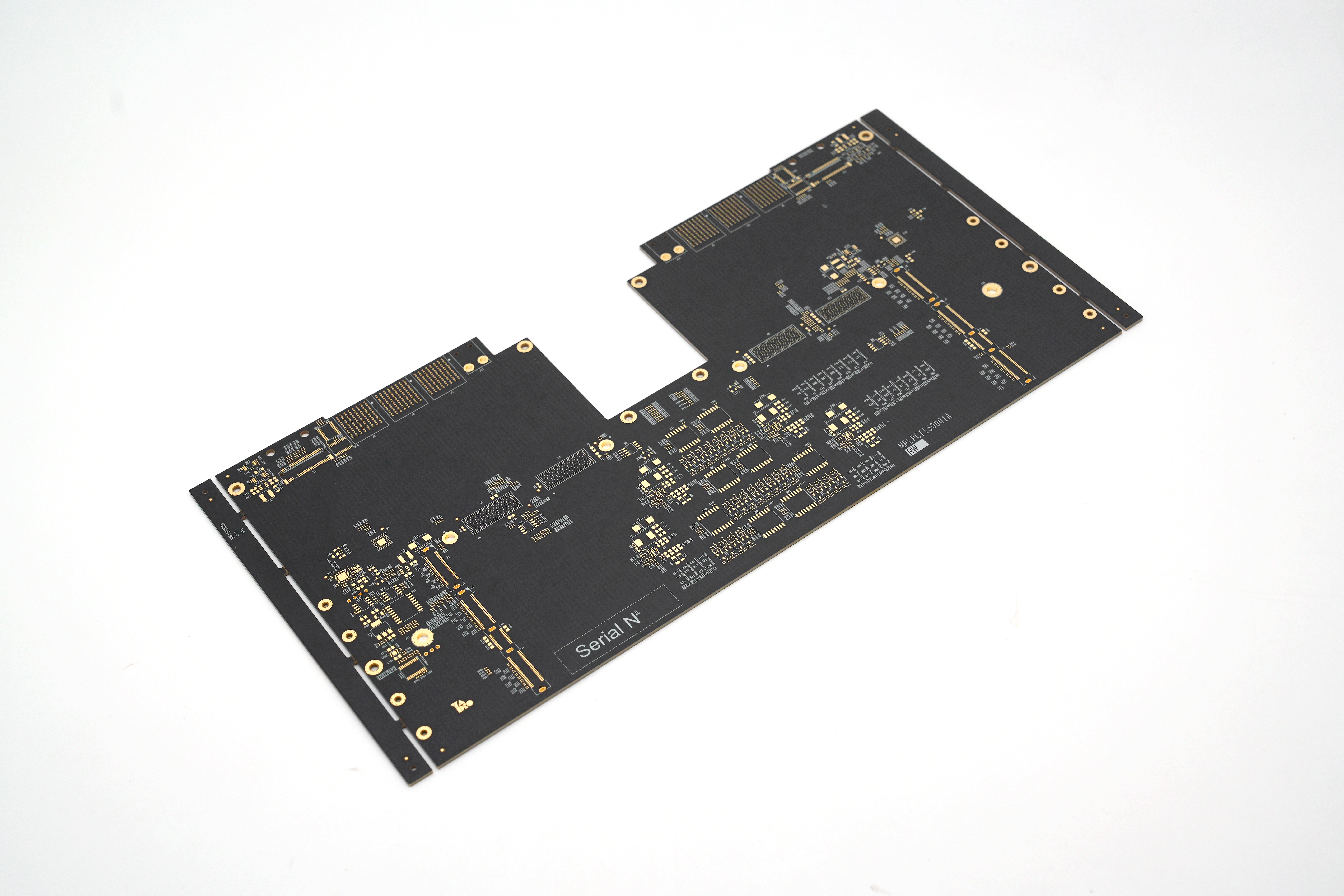
What is a high density PCB? Let’s discover pros and cons, application, layout technique, design guide and assembly processes for high density PCB board.
Are you troubled with these questions?
- Is your HDI design suffering from signal integrity issues that lower production yields?
- In high-frequency/high-speed scenarios, does thermal management on HDI boards compromise performance stability?
- Are complex HDI structures causing struggles with design validation during rapid iterations?
As a high density PCB manufacturer, EBest Circuit (Best Technology) can provide you service and solutions:
- Signal Integrity Analysis Service: Utilize advanced simulation tools to optimize routing design, reduce crosstalk, improve yields, and maximize space utilization for peak efficiency.
- Thermal Management Solutions: Integrate high-thermal-conductivity substrates with optimized cooling structures to tackle thermal challenges in high-frequency/high-speed applications, ensuring stable performance without additional layer stacking.
- Rapid Prototyping & Design Support: Provide quick-turn services from design to prototyping, complete complex HDI validation within 72 hours, accelerate time-to-market, and help you capture market opportunities first.
Welcome to contact us if you have any request for high density PCB board: sales@bestpcbs.com.
What Is A High Density PCB?
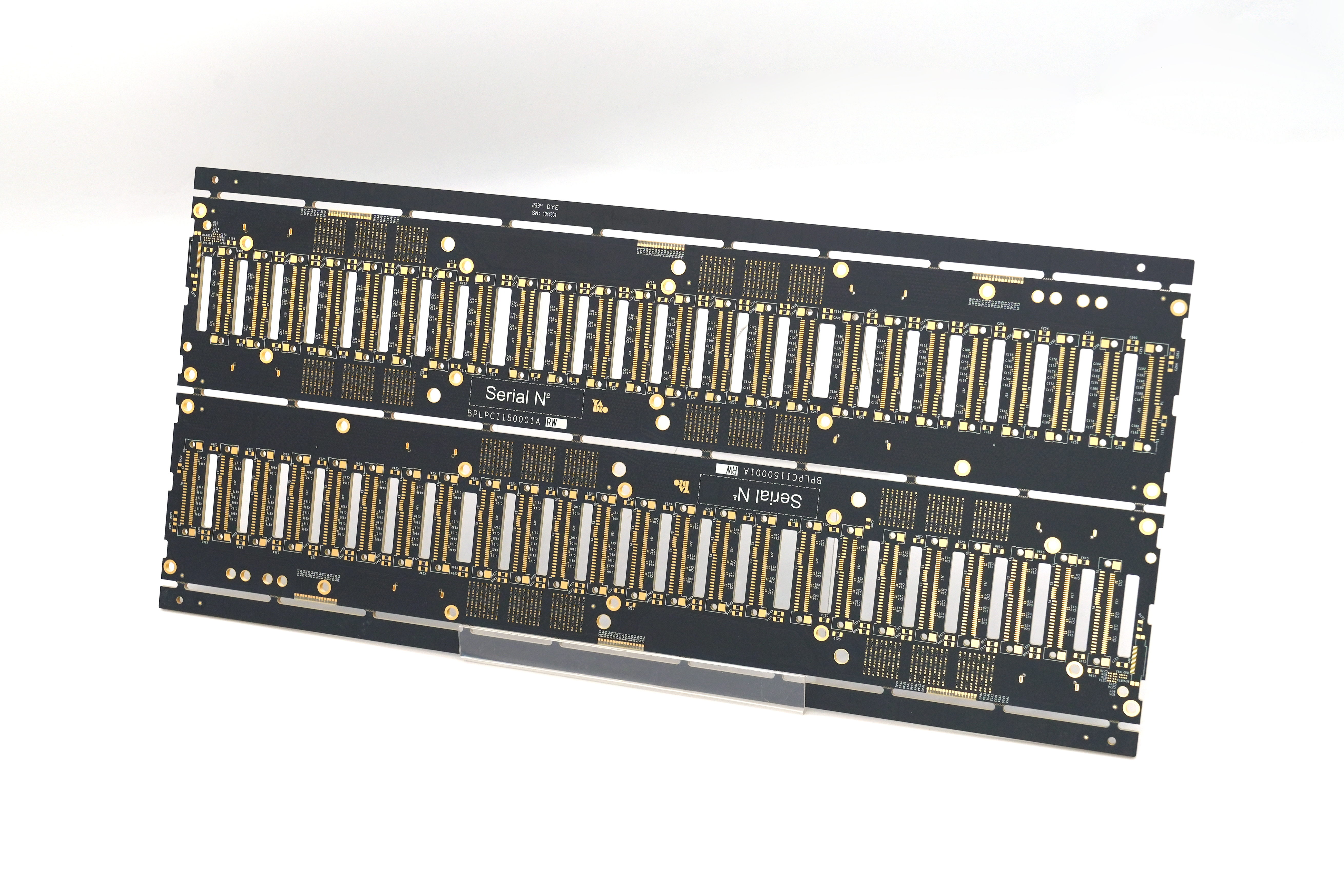
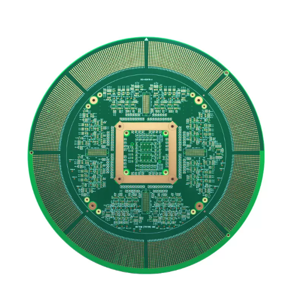
High Density PCB( High Density Interconnect Printed Circuit Boards) are PCBs fabricated using precision manufacturing technologies, with the core feature of integrating significantly more interconnect functionalities and components within a smaller physical space. This is primarily achieved through ultra-fine trace width/spacing (typically below 100µm/100µm), microvias with diameters often less than 150µm (e.g., laser-drilled holes), blind/buried via technologies, and increased routing layer counts.
HDI PCBs are designed to accommodate complex circuits and numerous high-density pin devices (such as BGAs and CSPs) within a compact area, meeting the stringent requirements of modern electronic products for miniaturization, lightweight design, high-speed operation, and enhanced performance.
What Are Pros of Cons of High Density Circuit Board?
Advantages of High-Density PCBs:
- Extreme Space Compression: Enabling complex circuits to be realized in a smaller area, meeting the dimensional sensitivity demands of wearable devices, micro-sensors, and other size-constrained end products.
- Enhanced Electrical Performance and Signal Integrity: Shorter routing paths reduce signal delay and crosstalk. Combined with microvias to minimize via stubs, this optimizes stability for high-speed/high-frequency circuits such as 5G and RF modules.
- High-Density Component Integration: Compatible with fine-pitch BGAs, CSPs, and SiP packages, addressing fan-out challenges for complex chips like FPGAs and multi-core processors while reducing transition layer counts.
- Weight Reduction: Fewer layers and substrate materials reduce overall weight, critical for aerospace, portable medical devices, and other applications with strict lightweight requirements.
- Increased Design Flexibility: Techniques like Every Layer Interconnect (ELIC) and blind/buried vias enhance routing freedom, supporting more complex topologies and design adaptability.
Disadvantages of High-Density PCBs:
- Significant Manufacturing Cost Increase: Laser drilling, specialty materials (e.g., low-Dk/Df dielectrics), and precision etching processes result in costs 30–100% higher than conventional PCBs, posing challenges for budget-sensitive projects.
- Design Complexity Surge: Stringent control of impedance consistency, signal return paths, and thermal planning is required. Reliability simulation for stacked microvias is difficult, extending design cycles.
- Yield Risks and Tight Process Tolerances: ≤50μm trace width/spacing demands high sensitivity to copper thickness uniformity and etching precision. Microvia copper plating voids increase, necessitating reliance on advanced equipment suppliers and complicating supply chain management.
- Design-for-Test (DFT) Limitations: High-density pads and buried components complicate test point placement, potentially requiring flying probe testing or custom fixtures, which escalate validation costs.
- Thermal Management Challenges: Increased power density per unit area restricts heat dissipation channels (e.g., limited space for thermal vias). Solutions like embedded copper blocks or thermal vias add design iterations and complexity.
What Are Applications of High Density Printed Circuit Board?
Applications of high density PCB board:
- Consumer Electronics: Smartphones, tablets, wearable devices (smartwatches, smart glasses), foldable phones, TWS earphones, etc.
- 5G Communication and RF Equipment: 5G base stations, RF modules, millimeter-wave communication equipment.
- Automotive Electronic Systems: Autonomous driving systems, in-vehicle infotainment, battery management, charging systems, ADAS, electric vehicle motor controllers.
- Medical Precision Equipment: Portable monitors, surgical instruments, implantable medical devices (pacemakers), ultrasound diagnostic equipment, minimally invasive surgical instruments.
- Aerospace and Defense: Flight control systems, navigation equipment, satellite communication modules, navigation and weapon control for fighter jets (e.g., F-35).
- Industrial Automation and Control: PLCs, sensors, industrial robots, automation equipment.
- Artificial Intelligence and Data Centers: High-speed server motherboards, AI computing modules, high-frequency circuits for data centers.
- Internet of Things (IoT) Devices: Smart homes, smart cities, environmental monitoring equipment.
High Density PCB Design Guideline
A detailed guideline to high density PCB design:
1. Layer Stack Structure and Material Selection
- Layer Count and Signal Layer Allocation: Determine the minimum layer count based on BGA/CSP component pin density and signal speed. For high-density scenarios, prioritize 2+N+2 or 3+N+3 symmetric stackups, separating power/ground planes from signal layers to reduce crosstalk. For example, 5G modules require at least 8-layer boards to ensure high-speed signal layers are isolated with adjacent reference planes.
- Material Parameter Control: Use low-Dk/Df (≤4.5/≤0.002) materials like Panasonic Megtron 6, aligning CTE (≤17ppm/°C) with copper to minimize warpage. Verify differential pair impedance (±10% tolerance) using 2D/3D field solvers (e.g., ANSYS SIwave).
2. High-Speed Routing and Crosstalk Mitigation
- Routing Rules: Prioritize manual routing for critical signals (e.g., DDR5, PCIe 4.0). Follow 3-4mil trace width/spacing rules (3/3mil in BGA fanout zones). Maintain differential pair spacing ≥2× trace width and length matching ±5mil. Keep high-speed trace spacing ≥3× trace width, cross-layer routing angles ≥30°, and add shielding vias (spacing ≤10mm) for sensitive signals.
- Via Optimization: Microvias (0.1-0.15mm diameter, aspect ratio ≤1:1) replace traditional through-holes. Via-in-pad requires resin filling + copper plating to prevent solder loss, validated by X-ray inspection (void ratio ≤5%).
3. Thermal Management and Heat Dissipation Path Design
- Thermal Structure Planning: QFN/DFN component thermal pad area ≥1.5× pin area. Deploy thermal via matrices (0.3mm diameter, 1mm spacing) under pads with ≥60% window ratio to balance thermal conduction and hermeticity. Place thermal via arrays (spacing ≤1.5mm) under power devices, connecting to inner thermal layers while avoiding BGA solder ball positions.
- Thermal Simulation Validation: Use ANSYS Icepak to simulate thermal distribution, ensuring junction temperature ≤125°C and key component temperature rise ≤30°C. Optimize heat diffusion paths via thermal via arrays and thermal layers.
4. DFM and Process Compatibility
- Pad and Solder Paste Design: Adhere to IPC-7351B standards. Pad size W_pad = W_lead + 2X + ΔD. Use elliptical pads (1.5:1 aspect ratio) for QFP components. BGA pad stencil aperture = 85% of pad diameter. Validate solder paste volume consistency via 3D SPI after printing.
- Panelization and Process Margins: Maintain ≥5mm process margins on board edges. Prohibit tall components in V-cut zones. Use slot + positioning hole designs for panelization to ensure SMT placement accuracy (±0.1mm). Confirm manufacturer capabilities (e.g., 4mil/4mil min trace/space) to avoid over-designing.
5. Signal and Power Integrity Co-Optimization
- Power Integrity Design: Implement power plane segmentation. Optimize decoupling capacitor (e.g., X7R/X5R) placement for high-frequency noise paths, matching capacitance values to signal speeds (e.g., 0.1μF + 10nF parallel for 100MHz). Connect power/ground planes via short vias to reduce impedance.
- EMI/EMC Solutions: Shield critical signals with shielding cases or conductive tapes. Use common-mode chokes for high-speed interfaces (e.g., USB 3.0). Validate radiated noise via near-field scanning to meet CISPR 32 standards.
6. Reliability Verification and Test Closure
- Electrical Testing: Flying probe tests cover all nets. Match impedance test frequencies to signal speeds. Validate microvia fill voids via X-ray (≤5%), AOI for pad shorts/opens, and ensure yield ≥99.5%.
- Reliability Testing: Thermal cycling (-40°C to 125°C, 500 cycles), random vibration (20g RMS), and solder joint reliability (3× reflow without cracks). Output Gerber/drill files, BOM, assembly drawings, DFM reports, and polarities (silkscreen width ≥0.15mm).
7. Cost Efficiency and Collaboration Optimization
- Cost Control Strategies: Use HDI substrates (e.g., 3+3+3 structure) in high-density zones, increasing cost by 30-50% while saving 40% space. For cost-sensitive projects, adopt staggered vias or embedded resistors/capacitors to reduce layers. Collaborate with manufacturers to obtain CPK reports (process capability index ≥1.33) for design-production alignment.
- Collaboration and Documentation: Implement version control via Git. Integrate Altium/Cadence EDA tools for constraint setup and simulation. Validate prototypes with Valor NPI or CAM350 DFM checks. Confirm manufacturer capabilities pre-production to avoid redesigns.
High Density PCB Layout Technique
Rational Layer Stack Planning
- Multilayer PCB Design & Layer Optimization: 6-10 layer PCBs dominate high-density applications. Increasing routing layers (signal, power/ground) enhances routing density and signal integrity. An 8-layer board typically employs a symmetric stackup like “signal-ground-power-signal” to suppress EMI and optimize impedance control.
- Thin Dielectric Materials & Impedance Matching: Low-dielectric-constant (Dk) thin substrates (e.g., 3-5mil FR4 or RO4350B) combined with microstrip/stripline structures enable precise impedance control (e.g., 50Ω single-ended, 100Ω differential). TDR testing verifies impedance continuity to prevent signal reflections caused by interlayer dielectric variations.
- Stackup Symmetry & Template Management: Utilize EDA tools (e.g., Altium Designer’s layer stack manager) to predefine symmetric stackup templates. Ensure core material and prepreg thicknesses and dielectric constants match to avoid board warping or signal distortion from asymmetric stackups.
Component Selection & Placement Optimization
- Compact Package Adoption: Prioritize 0201/0402 passive components (reducing footprint by >50%), BGA/CSP high-I/O packages, and fine-pitch QFN packages. For instance, 0201 capacitors save 20% board space while reducing parasitic inductance.
- High-Frequency & Sensitive Device Partitioning: Isolate RF modules, clock generators, and sensitive analog devices (e.g., ADCs, op-amps) from noise sources like DC-DC converters. Implement “thermal zoning” to cluster heat-generating components (e.g., power MOSFETs) near edge cooling areas.
- Vertical Space Stacking: Employ “stacked via” techniques under BGA pads, combining power/ground and signal layers vertically to save >30% routing space. For example, FPGA underfills with multi-layer buried vias achieve high-density interconnections.
Via & Routing Strategies
- Diverse Via Applications: Blind vias (connecting surface to inner layers), buried vias (connecting inner layers), and microvias (≤6mil diameter) shorten signal paths and reduce surface routing occupancy. Via-in-Pad with conductive fill reduces inductance and enhances signal integrity in BGA fanout regions.
- Differential Pair Optimization: Maintain equal length (length mismatch ≤5mil) and spacing (4-5mil) for differential pairs. Avoid crossing plane splits and use serpentine routing for length matching. Ground via fences isolate crosstalk, ensuring timing consistency for high-speed signals (e.g., PCIe, DDR).
Power & Ground Plane Management
- Ground Plane Partitioning & Single-Point Connection: Connect digital and analog grounds through beads or 0Ω resistors at a single point to prevent cross-coupled return paths. In mixed-signal systems, isolate analog and digital grounds, connecting only near power management ICs to reduce EMI coupling.
- Solid Copper Power Planes: Design power planes with ≥80% copper fill and multi-via arrays to enhance current capacity and thermal dissipation. For example, CPU core power regions use large copper areas with thermal via arrays to transfer heat to bottom-layer heat sinks.
- High-Frequency Decoupling Capacitor Placement: Position 0402/0202 decoupling capacitors (10nF-100nF) near high-frequency devices (e.g., oscillators, PLLs) with ≤5mm loop length to minimize power noise impact on sensitive circuits.
Signal Integrity & EMC Design
- High-Speed Routing Guidelines: Keep high-speed traces (clocks, differential pairs) ≥90mil away from plane edges to avoid crossing splits or via-dense areas. For DDR4 routing, equalize address/control line lengths using “flying trace” techniques to avoid bent signal paths.
- Shielding & Ground Via Arrays: Surround sensitive signals (e.g., RF traces, analog audio) with ground via arrays (spacing ≤100mil) to form Faraday cages, reducing radiated noise by >15dB (e.g., USB3.0 differential pairs with dual ground via shielding).
- Impedance Continuity & Trace Control: Use 4mil trace width/spacing and controlled dielectric thickness for 50Ω single-ended/100Ω differential impedance. Validate impedance curves with field solvers (e.g., Polar SI9000) to prevent distortion from process variations.
Thermal & Reliability Considerations
- High-Thermal Component Placement: Position power ICs, MOSFETs, and high-heat components near board edges or thermal vias. Use thermal via arrays (e.g., copper pillars, thermal pads) to transfer heat to top-layer heat sinks or metal enclosures. For LED driver boards, place power resistors near vents with thermal pads for efficiency.
- Thermal Stress Mitigation & Solder Pad Design: Apply HASL or OSP surface finishes in high-via-density areas (e.g., BGA pads) to prevent pad lifting or thermal stress. Expand solder pads by 10-20% to reduce capacitive effects and enhance solder reliability.
- High-Power Circuit Isolation: Separate power circuits (e.g., DC-DC converters) from sensitive circuits (e.g., analog front-ends) with isolation channels filled with high-Tg materials (e.g., FR4-Tg170) to enhance thermal stability.
Design Rules & Manufacturing Collaboration
- DFM Rules & HDI Process Adaptation: Define DFM rules (e.g., 4mil min trace/space, 6mil annular ring) aligned with HDI capabilities (laser drilling, sequential lamination). For BGA fanout, use “dog-bone” routing with microvias to connect pads to inner signal layers efficiently.
- EDA Tool Auto-Optimization: Leverage auto-optimization features in tools like Altium Designer (fanout, escape routing) for rapid BGA routing. Use interactive routing to adjust trace angles, avoiding impedance discontinuities from bent paths.
- Manufacturer Process Coordination: Confirm material selection (e.g., Rogers 4350B for high-frequency), process limits (0.1mm min via, 3mil trace/space), and surface finishes (ENIG, immersion gold) with PCB manufacturers. Balance cost-performance by selecting low-loss substrates for high-frequency designs to reduce signal attenuation.
High Density PCB Assembly Manufacturing Processes
1. Design Verification and DFM Analysis
- Signal integrity check: Use simulation software to verify impedance matching (±10% deviation), crosstalk suppression (controlled below 5%), and EMI/EMC compliance (meets CISPR 22 standards) for stable signal transmission in high-density layouts. Focus on critical traces (e.g., differential pairs, clock lines) topology optimization and termination resistor configuration to reduce reflections.
- Design for Manufacturability (DFM): Evaluate parameters like minimum trace width/spacing (≥3mil/3mil, HDI down to 2mil/2mil), via dimensions (microvia diameter ≤6mil, blind/buried via plating requirements), and pad shapes (e.g., QFN solder bridge prevention design) against process capabilities. Utilize DFM tools like Valor NPI for manufacturability analysis, optimizing layouts to reduce defects (e.g., minimizing heavy copper areas to prevent warpage, optimizing panel size for SMT efficiency).
- Thermal management design: Analyze component power distribution (e.g., CPU, power devices) and plan thermal channels (e.g., thermal via array density ≥10/cm?, thermal pad area ≥120% of component base). Use thermal simulation software like ANSYS Icepak to model heat flow, ensuring key areas stay below material Tg minus 10°C for thermal stability.
2. Material Preparation and Substrate Processing
- Substrate selection: Choose high-Tg materials (FR-4 High-Tg ≥170°C, polyimide ≥250°C) or high-frequency substrates (Rogers RO4350B, PTFE) for thermal stability and signal integrity. For rigid-flex boards, use low-modulus polyimide (Dupont Pyralux) for dynamic bending life (≥1 million cycles).
- Surface finish: Select surface treatments based on component type—OSP (organic solderability preservative for fine-pitch, 6–12-month shelf life), ENIG (electroless nickel immersion gold for edge connectors, Au ≥0.05μm/Ni ≥3–5μm), HASL (hot air solder leveling for cost efficiency, higher surface roughness), or immersion silver/tin (for high-frequency signals, surface roughness Ra ≤0.5μm). Ensure solderability and reliability, e.g., control nickel corrosion rate in ENIG to avoid black pad defects.
- Solder paste printing: Use laser-cut or electroformed stencils (opening accuracy ±5μm) to control paste thickness (3–8mil, thinner for micro-pitch). High-precision printers (DEK, EKRA) ensure uniform paste application for micro-components (01005, 0201). Calibrate print pressure/speed (e.g., squeegee pressure 1–3kg/cm, speed 20–100mm/s) and verify paste volume, area, height consistency (Cpk ≥1.3) via SPI equipment.
3. High-Precision Placement and Component Handling
- Placement machine setup: Use high-precision machines (Siemens SIP, Panasonic NPM) with vision systems (resolution ≤10μm, repeatability ±15μm) for 0201 components, BGA (0.4mm pitch), CSP, and high-density connectors (0.4mm pitch). Support multi-nozzle switching (e.g., 008004 component nozzles) and auto-calibration for mechanical error compensation.
- Component alignment: Achieve precise alignment (±25μm) via machine vision or laser systems. For BGA, use dynamic alignment to compensate for component warpage, ensuring ball-pad center alignment. For QFN/DFN, use specialized nozzles and placement algorithms (edge detection + pressure control) to prevent tombstoning or chip shift, with vacuum pressure monitoring for stable adsorption.
- Irregular component handling: For large components (connectors, inductors) or irregular packages (custom capacitors), use specialized nozzles and 3D vision for Z-axis height compensation. In high-density hybrid assembly, coordinate multi-station machines to optimize placement paths, reducing head movement time for efficiency.
4. Soldering and Curing Processes
- Reflow soldering control: Use nitrogen-purged reflow ovens (oxygen ≤50ppm) with multi-zone temperature profiles (preheat 120–150°C/90–120s, soak 150–180°C/60–90s, reflow 235–245°C/30–60s, cooling ≤4°C/s). Control peak temperature (235–245°C, 240±5°C for BGA) to prevent component/substrate damage. Monitor oven temperature via thermocouples/IR sensors, ensuring zone temperature differences ≤5°C. Use forced convection cooling for high-density boards to avoid local overheating.
- Selective soldering: For through-hole components (PTH pins) or localized high-density areas, use selective wave soldering or laser soldering. Wave soldering controls solder temperature (260–280°C), immersion time (2–5s), and wave height (5–10mm) to avoid bridging or voids. Laser soldering adjusts power (10–50W), pulse width (0.1–10ms), and spot size (50–200μm) for precision, suitable for micro-joints or heat-sensitive parts.
- Curing and inspection: Apply surface finishes via hot air leveling (HASL), UV curing (conformal coating), or IR curing (adhesives). Conformal coating uses automatic spray systems (PVA, Nordson) with controlled thickness (20–50μm) and uniformity (Cpk ≥1.5), ensuring no bubbles or sags. Post-cure, test curing degree (solvent wipe, DSC) for full cure and adhesion.
5. Inspection and Quality Control
- Automated Optical Inspection (AOI): High-resolution cameras (≥5μm pixel) detect solder defects (opens, shorts, insufficient/excess solder), component shifts, and polarity errors. AOI uses multi-angle lighting (ring, coaxial) for defect recognition, enhanced by deep learning for accurate classification (false call rate ≤0.1%). Generate detailed defect reports for rework or process optimization.
- X-ray Inspection: 2D/3D X-ray imaging inspects BGA/CSP under-ball joints for solder integrity (diameter deviation ≤10%), bridging, and voids (≤25% allowed). AXI requires high resolution (≤10μm pixel) and 3D imaging for internal quality assessment. For high-density packages, use tilted X-ray or CT scanning for comprehensive joint analysis.
- Flying probe/ICT testing: Flying probe testers (Takaya APT-1600) or ICT systems verify opens, shorts, and component value deviations (≤5%). Cover all critical nets and components for functional integrity. High-density boards use high-precision probes (≤0.1mm diameter) and adaptive algorithms for micro-pads and dense layouts.
- Functional testing and burn-in: Simulate real-world conditions with high-temperature burn-in (85°C/85% RH for 1000 hours), vibration testing (5–2000Hz, 1.5mm amplitude), and signal integrity checks (eye diagram, timing analysis). Burn-in monitors key parameters (leakage current, impedance changes) to screen early failures. Functional tests use test fixtures or ATE (Teradyne UltraFLEX) to validate full functionality, timing, and power integrity against design specs.
6. Special Processes and High-Density Techniques
- Blind/buried vias and microvia filling: Laser drilling (UV or CO?) and plating fill enable HDI designs. Laser drilling controls hole accuracy (±2μm) and wall roughness (Ra ≤1μm). Plating fill uses high-fill solder (Sn-Ag-Cu) and optimized parameters (current density, time) for void-free filling (≥95%). Microvias (≤6mil) use vacuum or pulse plating for better filling.
- Embedded copper blocks and thermal vias: Embed copper blocks (0.5–2mm thick) or thermal via arrays (≥10/cm?) in high-heat areas for optimized thermal paths. Thermal vias use solid copper fill or plating for high conductivity, verified by thermal simulation. For high-power components, combine thermal pads and vias for efficient heat dissipation.
7. Packaging and Final Testing
- Conformal coating application: Automatic spray or brush applies acrylic/polyurethane coating (20–50μm) for humidity, dust, and chemical protection. Pre-clean surfaces (plasma cleaning) for adhesion, then cure (thermal/UV) for performance. Coating must have low VOC and good weather resistance (salt spray, high-temperature/humidity tolerance).
- Final functional validation: Test fixtures or ATE (Keysight 3070) verify full functionality, signal timing, and power integrity. Cover all key modules (processor, memory, power management) with eye diagram and timing analysis for signal quality. For high-reliability products, perform environmental stress screening (temperature cycling, vibration) to eliminate latent defects.
- Packaging and traceability: Use anti-static packaging (conductive bags, foam) to prevent ESD damage. Attach barcode/QR labels for traceability (component batches, process parameters, inspection results). Integrate with MES for real-time data updates and query access. Final inspection checks for scratches, deformation, and packaging integrity before shipment.
Why Choose EBest Circuit (Best Technology) as High Density PCB Manufacturer?
Reasons why choose us as high density PCB manufacturer:
- 19-Year Industry Experience & Technical Accumulation: With 19 years of focused expertise in high-density PCB manufacturing, we accumulate extensive process databases and case libraries. This enables rapid identification and resolution of complex design issues, providing clients with mature and reliable production solutions.
- International Authoritative Certification System: Hold ISO 9001 quality management, IATF 16949 automotive, medical-grade, and RoHS environmental certifications. These meet compliance requirements for high-demand sectors like automotive electronics, medical devices, and industrial controls, aiding client products in global market access.
- Free DFM (Design for Manufacturability) Analysis: Offer free professional DFM analysis services. Before production, optimize design details and identify/rectify potential manufacturing risks (e.g., excessively small trace widths/spacings, improper pad designs) to reduce trial production failure rates and save clients secondary sampling costs.
- Cost Competitiveness & Customized Solutions: Deliver industry-leading price advantages paired with cost-sensitive design schemes. Through material optimization, process refinement, and scalable production, we help clients significantly reduce per-board costs while maintaining performance, particularly for budget-sensitive batch orders.
- 24-Hour Expedited Prototyping Service: Address urgent project needs with a 24-hour rapid prototyping commitment. This shortens prototype validation cycles, accelerates product launch timelines, and safeguards R&D progress to prevent market opportunity losses due to sampling delays.
- 99.2% On-Time Delivery Rate: Leverage efficient supply chain management and production scheduling systems to ensure 99.2% of orders are delivered on time. This reduces client production downtime risks from delivery delays and enhances supply chain reliability and predictability.
- Strict Quality Control & Batch Full Inspection: Implement full-process quality control from raw materials to finished products. Batch orders undergo 100% full inspection, integrating electrical performance testing, and multiple quality verification methods to ensure defect rates below industry averages and high product reliability.
- Production Error Database-Driven Cost Optimization: Utilize a production error database for historical issue attribution analysis. This proactively avoids common design or process defects, reduces rework and scrap costs, directly lowering clients’ hidden costs by 3%-5%, and boosts production efficiency.
- Flexible Production Capacity & Rapid Response Capability: Equip multiple automated production lines and intelligent warehousing systems to support seamless switching from small to large batch production. This swiftly responds to client demand changes, showcasing significant cost and time advantages, especially for multi-variety, small-batch orders.
- Full Lifecycle Technical Support: Provide comprehensive technical support from design consultation, production tracking, to post-sale issue resolution. A 24/7 technical team ensures clients receive professional guidance across R&D, production, and post-sale stages, maximizing client investment returns.
How to Get a Quote for HDI PCB Board Project?
High Density PCB Project Quote Request Checklist:
- Design Files: Gerber files (must include layers, solder mask, silkscreen); PCB layout files (e.g., Altium, Eagle, OrCAD)
- Bill of Materials (BOM): Component list with part numbers, specifications, and quantities
- Technical Specifications: Layer count, thickness, material type (e.g., FR4, Rogers), copper weight; Surface finish (e.g., ENIG, HASL, OSP); Minimum trace width/spacing, via size (e.g., 100µm/100µm, microvias)
- Special Requirements: Impedance control requirements (e.g., 50Ω traces); Blind/buried vias, HDI (High Density Interconnect) features; High-frequency materials (e.g., Rogers 4350), thermal management needs
- Production Details: Quantity (prototype/small batch/mass production); Lead time expectations (e.g., 3-day quick-turn, 10-day standard)
- Testing & Certification: AOI/X-ray inspection, flying probe testing; Certifications (e.g., UL, IPC-A-610 Class 3);
- Contact Information: Company name, contact person, email, phone number.
Welcome to contact us if you have any inquiry for high density PCB board: sales@bestpcbs.com.