

What is ICT tester? Let’s explore its components, pros and cons, function, working principle, detection type, difference between flying probe.
Are you worried about these questions?
- Is production line testing slowing you down? How to handle slow delivery and high costs for large orders?
- Can’t afford testing for small batches? Unit costs exceed budget, eating into your profits?
- Design changes causing delays? Fixture rework takes 2-4 weeks, stretching your timeline?
As a PCBA service supplier, EBest Circuit (Best Technology) can provide you service and solution:
- Dual-Mode Acceleration: Combine flying probe and ICT for 2000-point testing in 2 seconds, cutting delivery time by 40%!
- Cost Reduction: Modular programming and dynamic mapping slash unit costs by 80% for small batches!
- Fast Design Changes: Automated program adaptation completes test adjustments in 72 hours—no production stoppages!
Welcome to contact us if you have any request for PCBA service: sales@bestpcbs.com.
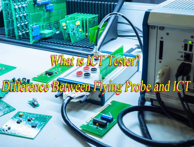
What is an ICT Tester?
ICT Tester( also called as in-circuit tester) is an automated device that utilizes a precision needle bed fixture to directly contact test points on a printed circuit board (PCB). Operating in a non-powered or component-isolated state, it rapidly detects assembly defects.
It is primarily used to identify physical faults such as solder shorts, opens, component misplacement or missing, and parameter value deviations, accurately pinpointing problem locations. As a critical testing tool in the electronics manufacturing process, it ensures the reliability of fundamental electrical connections on PCBs.
What Are Components of In-Circuit Tester?
Components of In-Circuit Tester:
- Test Circuitry: Includes control circuits and switching circuits. The control circuit is responsible for testing component parameters (such as resistance, capacitance, and inductance). The switching circuit is used to connect the components to be tested and is typically composed of relays or CMOS semiconductor switches.
- Computer and Software System: Most sources mention that the ICT system includes a standard PC running the Windows operating system and ICT test software, which is used to control the test process, display results, and generate statistical data. The software also includes test programs, data analysis, and fault diagnosis modules.
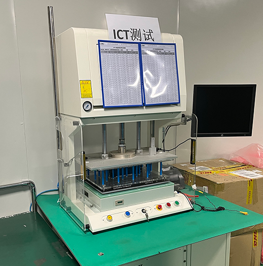
- Mechanical Transmission and Pneumatic Systems: These include pneumatic clamps, limit switches, and vacuum chambers. The pneumatic clamp is driven by compressed air to press or lift the circuit board. The limit switch controls the downward position. The vacuum chamber may be used to secure the PCB or provide a vacuum environment.
- Power Supply System: Includes a programmable DC power supply (such as the HP6624) to power the test head and the PCB under test. It may also include a modular power supply (MPU) and a DUT power supply, providing different voltages and currents.
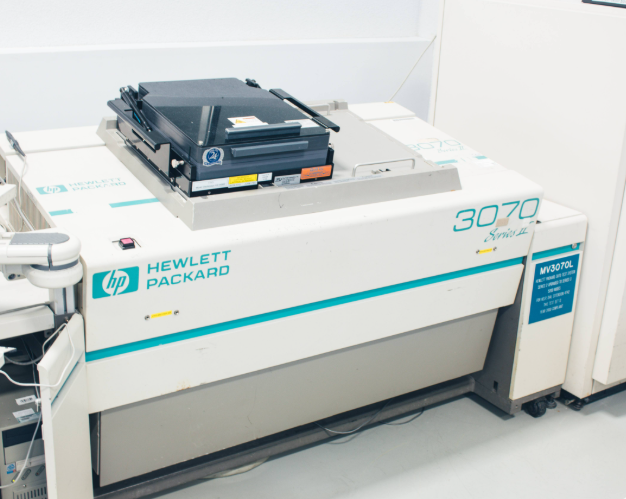
- Test heads and modules: For example, Agilent ICT test heads consist of the testhead, controller, and support bay. They feature a modular design, including ASRU cards (Analog Stimulus Response Units), control cards, and pin cards. Each module is responsible for a specific test function.
- Signal sources and measuring instruments: These instruments generate test signals (such as sine waves and pulses) and measure responses, including voltage comparators, D/A converters, A/D converters, and signal conditioning cards.
- Isolation technology: Voltage followers or isolation circuits designed with operational amplifiers prevent interference from other components during testing, ensuring accurate measurement of the DUT.
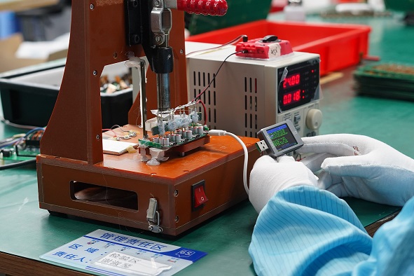
- Auxiliary components: These include probes (test needles), fixtures, induction boards (for TestJet testing), electrostatic protection materials (such as ESD bakelite), and counters (for recording test times).
- Data interfaces and communications: These include serial communication interfaces (such as RS-232) and GPIB interfaces, used to connect computers and test equipment to transmit control commands and test data.
What Are Pros and Cons of ICT Tester?
Pros of ICT Tester:
- High Coverage: Detects component connections and soldering defects on PCBs with extremely high coverage (typically approaching 100%).
- High Speed: The testing process is highly automated, typically completing a PCB test in seconds to tens of seconds.
- High Precision: Direct access to test points and electrical isolation technology ensure high measurement accuracy.
- Precise Defect Location: Can clearly pinpoint which component or pin has a specific type of defect (e.g., an open resistor or a poor solder joint on pin 5 of an IC), greatly facilitating repairs.
- High Defect Detection Rate: High detection capabilities for common physical defects introduced during the manufacturing process (open/short circuits, missing/missing components, and poor soldering).
- Suitable for High-Volume Production: Its high speed and high degree of automation make it ideal for high-volume testing on production lines.
Cons of Tester:
- High Fixture Cost: Custom bed-of-nails fixtures are time-consuming and expensive to develop, especially for complex, high-density boards.
- Test Point Dependency: Sufficient, accessible test points must be reserved during the PCB design phase. High-density designs (such as HDI boards and boards with many BGA components) make it difficult to place sufficient test points.
- Limited test coverage: Testing primarily tests static parameters and connectivity, but cannot verify circuit functionality and dynamic performance (such as clock frequency, signal integrity, and software operation). Functional testing capabilities for complex ICs are limited.
- Programming complexity: Developing efficient and comprehensive test programs requires expertise and time.
- Contact reliability: The quality of contact between the probe and the test point is critical; contamination, oxidation, and probe wear/deformation can affect test results.
- Device limitations: Devices that require power to operate (such as coils, relays, and some sensors) or devices completely enclosed in shielded enclosures cannot be tested.
What is the Function of ICT Tester?
Function of ICT Tester:
- Connectivity Testing: Uses test probes to contact circuit board points, rapidly identifying open/short circuits and verifying correct signal path connectivity.
- Component Parameter Verification: Precisely measures electrical parameters (e.g., resistance, capacitance, inductance, voltage) of components (resistors, capacitors, diodes, transistors) against standards to detect out-of-tolerance parts.
- Functional Logic Validation: Simulates real-world operating conditions, injecting test signals to validate output responses of functional modules (ICs, optocouplers, power supplies) per design specifications.
- Process Defect Screening: Automatically detects welding issues (cold solder, missing solder, solder bridges), component misalignment, pin lift, and PCB trace breaks to prevent defective units from advancing.
- Polarity Verification: Employs dedicated techniques (e.g., third-pin excitation + spectrum analysis) to confirm correct polarity of electrolytic capacitors and parallel capacitor alignment.
- Integrated Circuit Specialized Testing: Supports functional testing of small/medium-scale ICs (logic chips, drivers) and memory devices (EEPROM/FLASH) to detect programming errors or anomalies.
- Automated Testing & Data Management: Enables fully automated testing via pre-programmed sequences, generating test reports with fault locations, measured values, and standards in 1–several seconds per board. Supports statistical analysis.
- Fault Localization: Pinpoints specific faults (e.g., resistor deviation, capacitor failure, IC pin contact issues) to reduce repair dependency on expertise and accelerate troubleshooting.
- Process Optimization: Analyzes defect data (e.g., solder bridge rate, component missing rate) to trace root causes (operator error, equipment precision) and drive process improvements.
- Safety & Cost Control: Utilizes low-current/voltage static testing to prevent component burnout; early defect detection reduces repair costs (production-end fault costs are ~1% of user-end costs per studies).
How Does an ICT Tester Work?
1. Test Preparation
- Test Point Design: During PCB design, standardized test pads/vias (diameter 0.8-1.2mm) are reserved. High-density boards use “flying probe test points” to avoid signal interference, while high-current paths require widened test points to reduce contact resistance. For example, mobile phone motherboard test points maintain 50-150g pressure for reliable contact without damaging pads.
- Program Development Logic: Test scripts are written using software like Teradyne/Keysight, based on Gerber files or schematics. Thresholds account for component tolerance stacking—e.g., a 100Ω±5% resistor sets 95-105Ω as the pass range, triggering alarms for deviations.
- Positioning Technology: PCBs are secured via pneumatic/vacuum fixtures. Probe arrays use CCD vision calibration for micrometer-level contact accuracy, ensuring precise alignment with test points.
2. Open/Short Test
- Low-Voltage Pulse Detection: 1-10V pulses are injected into test points. Short circuits are detected via “star-resistance network” algorithms identifying unintended network connections. Open circuits are judged by “conduction resistance thresholds”—e.g., a line with 50mΩ standard resistance is flagged as open if measured >1Ω.
- Defect Traceability: A power path with abnormal high resistance triggers automatic backtracking to the nearest solder joint. Combined with X-ray inspection, voids or cold solder are identified, reducing debugging time from hours to minutes.
3. Component-Level Test
- Categorized Detection: Resistors use 4-wire Kelvin measurements to eliminate lead resistance; capacitors are tested via LCR meters for capacitance/loss angle; inductors are checked for Q-factor/DCR; diodes verify forward voltage/reverse breakdown; transistors test DC gain/leakage. For instance, a 0.1μF capacitor measured at 85nF (15% deviation) is rejected.
- Dynamic Threshold Adjustment: Temperature-sensitive components (e.g., thermistors) auto-compensate for ambient temperature. Threshold libraries update dynamically during mass production to address parameter drift, maintaining strict quality control.
4. Functional Test
- Chip-Level Verification: MCUs/FPGAs undergo JTAG boundary scan or analog stimulus to validate logic functions. A processor must pass “instruction set integrity tests” ensuring all registers/interfaces operate correctly.
- Power Module Dynamic Testing: Modules are tested under full/no-load and transient conditions for voltage ripple, efficiency, and overcurrent protection. A server PSU demonstrated <2% voltage fluctuation during 10ms load transitions, confirming robust dynamic response.
5. Result Analysis & Repair
- Intelligent Fault Reporting: Detailed reports include defect coordinates, component IDs, and fault types (open/short/parameter out-of-spec), linked to BOM/process data. For example, a failed C101 capacitor auto-flags its supplier batch for traceability.
- Repair Workflow: Technicians replace components/repair joints using precision tools based on reports. Post-repair retesting ensures full fault resolution. Statistics show ICT reduces downstream functional test failures by >80%, boosting production yield.
What Types of Defects Can the ICT Tester Detect?
1. Connectivity Defects
- Detection Scope: Open circuits, short circuits, broken wires, interlayer shorts/breaks in PCBs.
- Technical Principle: Micro-power signals are applied to test points via probe contacts to verify connectivity. For instance, four-wire resistance measurement precisely locates broken wires, while AC signals detect unintended shorts between adjacent traces.
- Case Example: Misaligned positioning holes post-PCB lamination causing surface-to-surface wire breaks are rapidly pinpointed by ICT.
2. Component Parameter Defects
Detection Range: Parameter deviations in resistors, capacitors, inductors, diodes, transistors, optocouplers, and ICs.
Technical Details:
- Resistors: Current injection and voltage measurement for resistance calculation (e.g., a 10kΩ resistor measuring 500Ω due to parallel resistance interference).
- Capacitors: AC signal-based capacitance measurement for small values; DC charge/discharge analysis for large capacitors (e.g., 40,000μF capacitor curve analysis).
- IC Pins: Forward/reverse voltage scanning of VCC/GND pins to identify soldering defects like cold joints.
3. Soldering Process Defects
Typical Issues: Solder bridges, component misplacement/reversal, lifted leads, voids, BGA solder ball shorts.
Innovative Techniques:
- Voltage Sensing: Surface pads detect pin bonding strength (e.g., signal attenuation in open-soldered IC pins).
- Boundary Scan (IEEE 1149.1): TDI/TMS/TCK/TDO signal links enable deep-pin testing without probes (e.g., U3 driving U1 to validate R1 soldering).
4. IC Functional Defects
Detection Targets: 74-series logic chips, memory modules, driver ICs.
Testing Methods:
- Vector Testing: Digital sequence input to verify logic outputs (e.g., pin interconnection signal response analysis).
- Functional Simulation: Power module stability under simulated inputs; op-amp gain error validation.
5. Polarity-Related Defects
- Key Cases: Reversed electrolytic capacitors, misoriented diodes, transistor pin misconnections.
- Technical Advances: DSP-based FFT spectral analysis with trigger signals on third pins for polarity verification (e.g., top-signal vs. anode/cathode reaction in capacitors).
6. LED Performance Defects
Metrics: Color deviation, uneven illumination, insufficient brightness, flickering, protocol failures.
Advanced Solutions:
- Fiber-Optic Spectrometers: Spectral composition and total flux measurement (e.g., T100L tester for micro-spot analysis across hundreds of LEDs).
- Flying Scan: Overcomes multi-chip LED interference for precise single/multi-chip module characterization.
7. Process-Induced Defects
- Problem Types: Missing components, wrong parts, PCB opens, test-point oxidation, fixture drilling inaccuracies (e.g., ±20μm tolerance control).
- Solutions: Learning-value comparisons (e.g., resistance tolerance bands T+/T-) and statistical fault localization (e.g., identifying R1 as the highest-failure component in a batch).
8. Dynamic Functional Defects
- Detection Scenarios: Post-power-on functional anomalies like power module ripple, digital timing errors.
- Implementation: Automated test programs simulate operational conditions with GPIB-integrated devices (e.g., Keithley 2000 multimeter for 0.1μV-1000V DC measurements).
9. Packaging & Structural Defects
- Special Cases: BGA solder ball shorts, bottom-terminated component (BTC) solder integrity, shielding effects from metallic enclosures (e.g., signal attenuation on chip surfaces).
- Countermeasures: X-ray inspection complemented by ICT; parallel PN-junction detection to bypass metallic shielding.
10. System-Level Defects
- Integrated Detection: Multi-device interconnection faults (e.g., open-soldered parallel IC pins); coverage of nodes without test points via hybrid boundary scan + voltage sensing.
- Data Value: Test results traceable to production batches for root-cause analysis (e.g., operator errors vs. PCB layout flaws causing thermal stress cracks).
What is the Difference between a Flying Probe and ICT?
Test Principles and Equipment
- Flying Probe Test: Utilizes XYZ three-axis precision servo platforms with 20μm-diameter probes (ruby/tungsten-coated), integrated optical positioning (±5μm accuracy), vacuum adsorption platforms, and supports non-contact capacitance testing. Suitable for HDI boards, 3D-MID, and other irregular PCBs.
- ICT Test: Combines needle-bed fixtures with spring probe arrays (lifespan >500,000 cycles), integrates boundary scan (JTAG) technology, and can form an “optical + electrical” dual-verification system with AOI.
Flexibility and Adaptability
- Flying Probe Test: Dominant in R&D stages (e.g., automotive electronics BGA embedded capacitor testing). Program adjustments are plug-and-play, with rapid response to design changes (monthly frequency >3 times). For small-batch medical devices (<500 pieces/year), it saves 80% fixture costs.
- ICT Test: Dominates mass production (e.g., iPhone PCB lines testing 1,200 pieces/hour with 3-year fixture lifespan). Achieves 99.9% yield in power module testing but requires 2-4 weeks to redevelop fixtures for design changes.
Test Speed and Efficiency
- ICT: Excels in parallel testing, completing 2,000 test point contacts in 2 seconds.
- Flying Probe Test: Single-board test takes ~2 minutes (60x slower), but high-density boards (50μm line width) can reduce to 30 seconds via multi-probe synchronization.
Cost Structure
- Flying Probe Test: Equipment costs ¥500,000–2,000,000, per-piece testing cost ¥1–5, ideal for annual volumes <5,000 pieces.
- ICT Test: Fixture development costs ¥100,000–500,000, per-piece cost <¥0.1, with significant total cost advantages for volumes >100,000 pieces.
Test Coverage and Capabilities
- ICT: Detects shorts/opens, capacitor tolerance (±1%), inductor Q-value, supports boundary scan chain testing, and direct contact with power planes.
- Flying Probe Test: High precision for passive components (e.g., 0201 resistors ±0.5%) but requires functional testers for complex logic functions.
Applicable Scenarios
- Flying Probe Test: Aerospace prototype validation, rapid adaptation of new energy battery management systems, small-batch high-reliability PCB testing.
- ICT Test: Mass production in smart home appliances and industrial controls (e.g., air conditioner boards with annual output >1 million pieces), integrated with MES for quality traceability.
PCB Design Requirements
- ICT: Requires test point spacing ≥0.5mm, concentrated at edges to reduce fixture costs; Altium and other tools support automatic layout optimization.
- Flying Probe Test: No strict test point design requirements, but high-density designs must consider probe accessibility (e.g., avoiding shielding by large components).
Technological Trends
- Flying Probe Test: Evolving toward “4D”, higher precision (probes ≤15μm), faster speed (≥500mm/s movement), higher density (>16 probes), and AI-driven defect classification.
- ICT Test: Focused on “3C”, modularization (quick-swap modules), integration (functional test + AOI), and greening (reduced fixture wear).
Welcome to contact us if you have any other issues about difference between flying probe and ICT: sales@bestpcbs.com.
You may also like

Tags: flying probe vs ict, ict tester, ICT Testers