

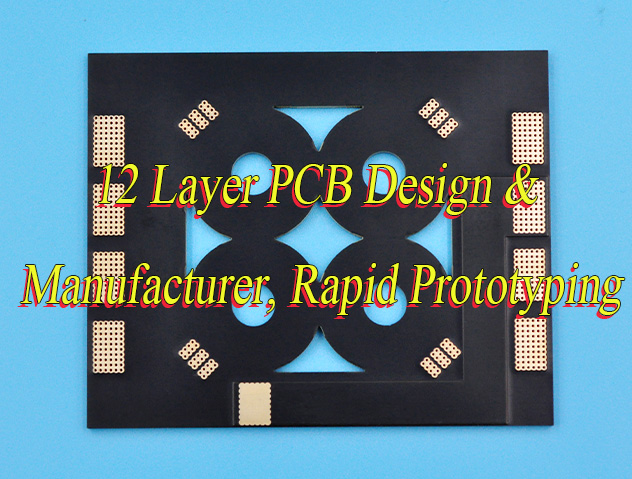
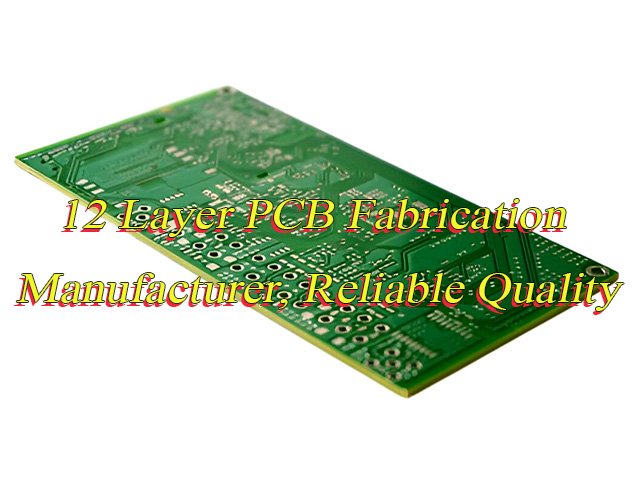
What is 12 Layer PCB? Let’s explore thickness, stackup configuration, design spec, design guide, lead time, cost for 12 layer PCB.
Are you worried about these problems?
- How to resolve the dual challenge of “signal layer crosstalk” and “EMI exceedance” in 12-layer PCB design?
- During multi-layer PCB manufacturing, how to prevent “laminate misalignment” from causing shorts/opens and ensure first-pass yield?
- When research cycle is compressed to 3 weeks, how to achieve the perfect balance of “rapid prototyping” and “quality control”?
As a 12 layer PCB manufacturer, EBest Circuit (Best Technology) can provide you services and solutions:
- Design Empowerment: Free DFM (Design for Manufacturing) analysis + signal integrity simulation, delivering optimized reports within 3 days to minimize design revisions and ensure first-time success.
- Process Guarantee: Utilizing imported high-precision laminators with layer-to-layer alignment accuracy ≤0.05mm, complemented by AI-powered visual inspection to eliminate “hidden cracks” and ensure robust quality.
- Speed Advantage: Standard prototyping delivered in 5 days, with emergency orders supported by a “green channel” for 24-hour progress tracking.
Welcome to contact us if you have any request for 12 layer PCB: sales@bestpcbs.com.
What is 12 Layer PCB?
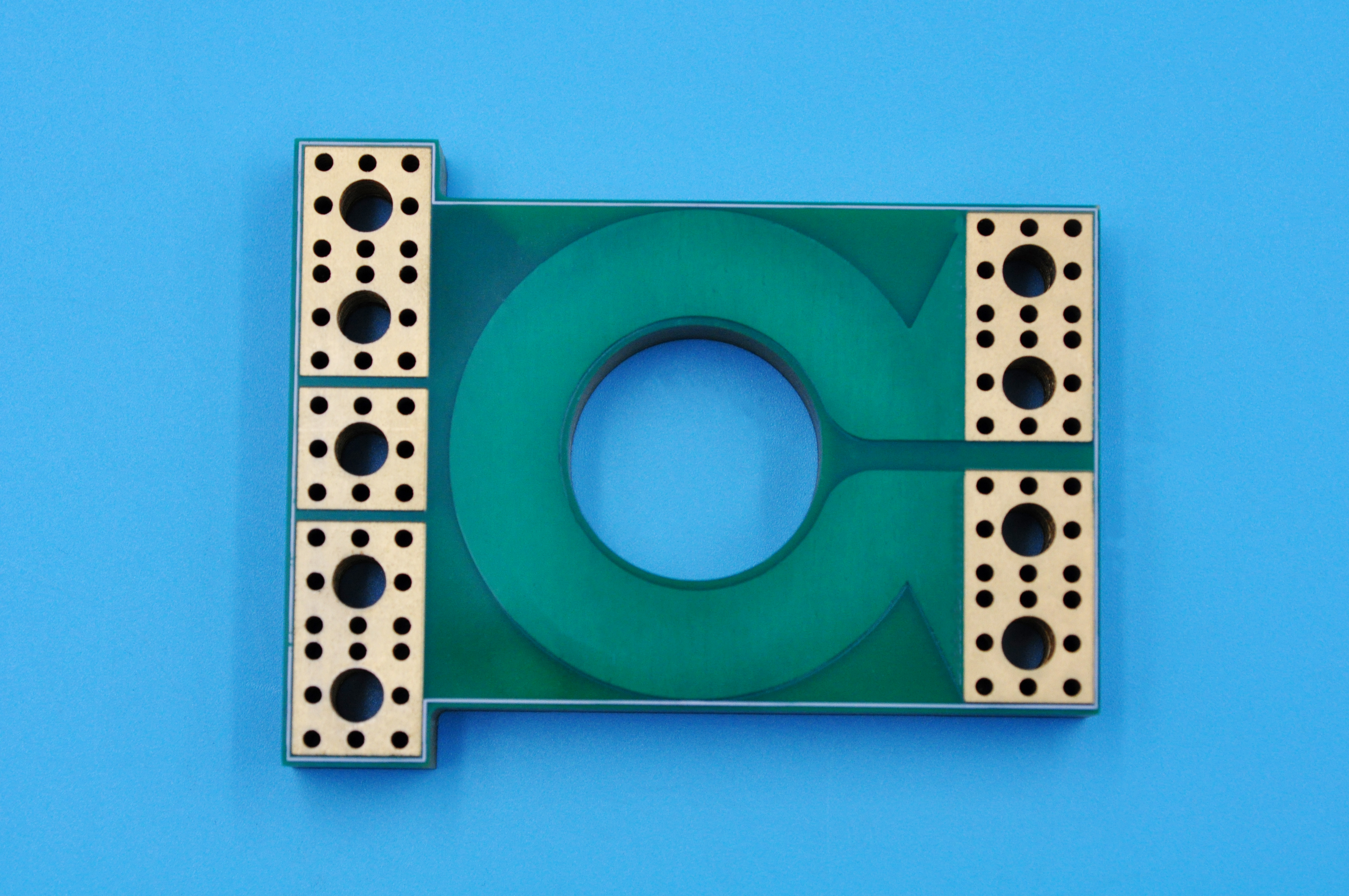
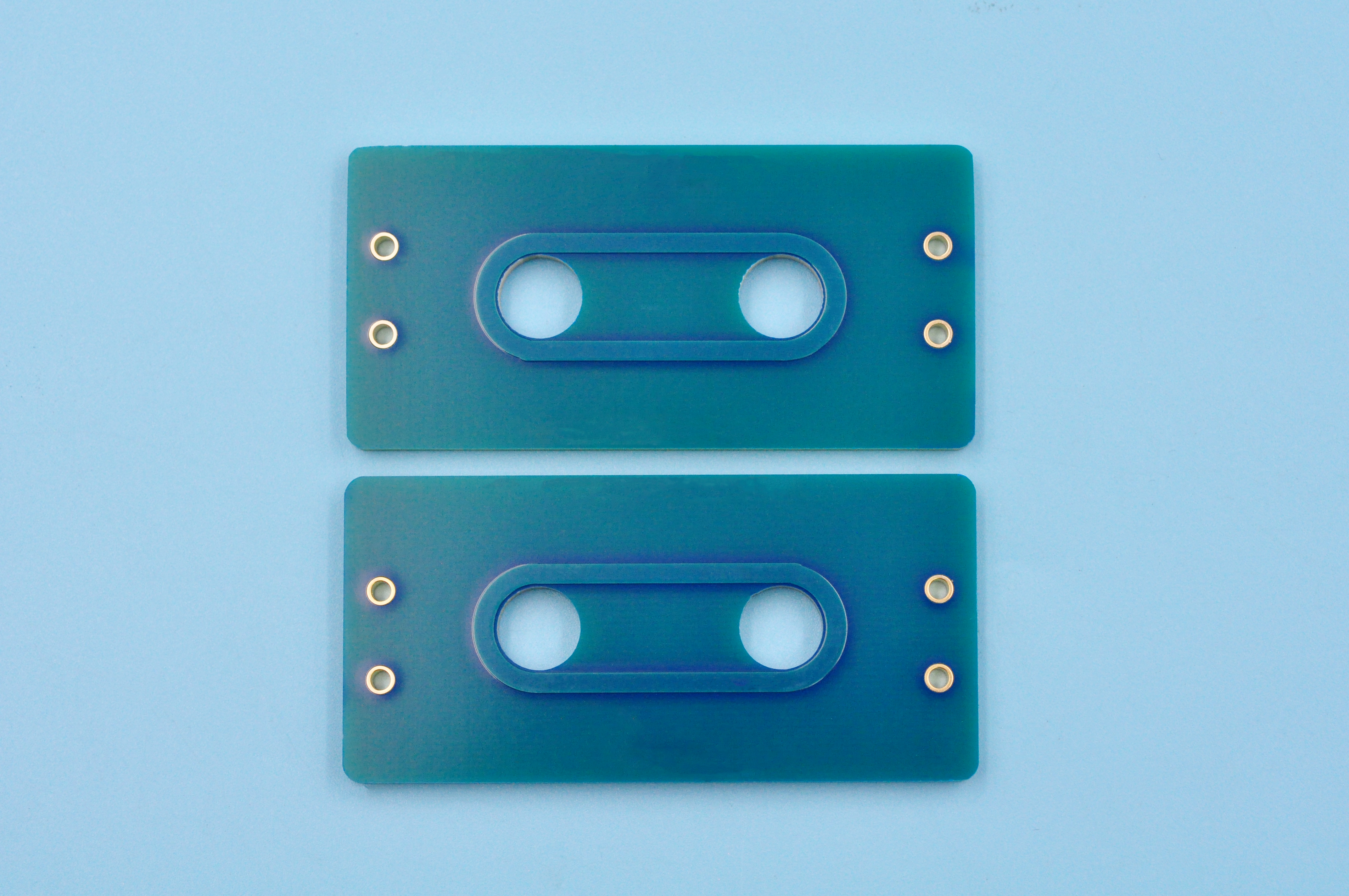
A 12 layer PCB (12-Layer Printed Circuit Board) is a multilayer printed circuit board composed of 12 layers of conductive copper foil alternately laminated with insulating substrates. Its core design is realized through a precision laminated structure: typically incorporating multiple signal transmission layers, power layers, and ground layers. These layers are separated by ultra-thin insulating materials and vertically interconnected via vias formed through laser drilling and plating processes.
This architecture significantly enhances circuit complexity and routing density within limited space, while dedicated layers enable high-speed signal shielding, power noise suppression, and electromagnetic compatibility (EMC) optimization. Primarily applied in high-performance, high-reliability, and complex-function domains (e.g., 5G base stations, AI servers, high-end industrial control equipment), it serves as a key technical solution balancing circuit integration and electrical performance.
How Thick is a 12 Layer PCB?
The actual thickness of a 12-layer PCB is typically between 1.5mm and 1.6mm, depending on the manufacturer’s process and design requirements. According to PCB standard thickness specifications, 12-layer boards can support thicknesses from 0.4mm to 4.5mm; however, in conventional high-performance scenarios, a tolerance control of 1.57mm ±10% is often adopted to balance circuit integration and electrical performance.
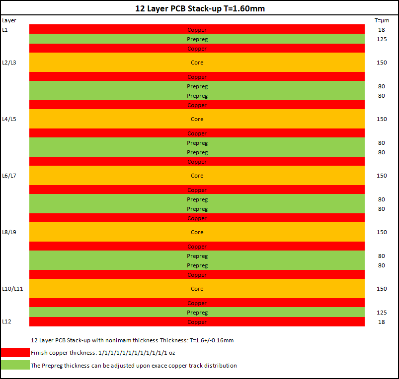
12 Layer PCB Stackup Configuration
Standard High-Speed Design (8S2P2C)
- Top(S1) – Prepreg – Inner(C1/GND) – Core – Inner(S2) – Prepreg – Inner(S3) – Core – Inner(PWR1) – Prepreg – Inner(S4) – Core – Inner(S5) – Prepreg – Inner(PWR2) – Core – Inner(S6) – Prepreg – Inner(C2/GND) – Bottom(S7)
- Note: 8 signal layers + 2 power layers + 2 ground layers, symmetric structure, optimized for impedance control.
Enhanced Power Integrity (6S4P2C)
- S1 – PP – C1 – Core – S2 – PP – PWR1 – Core – PWR2 – PP – S3 – Core – S4 – PP – PWR3 – Core – PWR4 – PP – C2 – S5
- Note: 6 signal layers + 4 power layers + 2 ground layers, suitable for multi-voltage domains and high-current scenarios.
Ultra-Thin Dense Routing (8S4C)
- S1 – PP – C1 – Core – S2/S3 (adjacent signal layers) – PP – C2 – Core – PWR1 – PP – C3 – Core – S4/S5 – PP – C4 – Core – S6 – PP – S7
- Note: 8 signal layers + 4 ground layers, no dedicated power layers (power distributed via copper pour), thickness compressible to 1.2mm.
12-Layers PCB Design Specification
| Technical Parameter | Standard Value/Range |
| Stackup Structure Type | 8S2P2C / 6S4P2C / 8S4C |
| Single-Ended Signal Impedance | 50Ω ±8% |
| Differential Pair Impedance | 85Ω / 100Ω |
| Interlayer Dielectric Thickness | 0.17mm – 0.2mm |
| Copper Foil Thickness | Inner layers: 1oz; Outer layers: 1-2oz |
| Material Selection | FR-4 (General) / Megtron 6 / TU-872 SLK (High-Speed) |
| Power Integrity | Power-Ground Plane Spacing ≤10mil |
| Thermal Management | High-Thermal-Conductivity Substrate (e.g., Metal Core) |
| Signal Integrity Measures | Differential Pair Length Matching / Impedance Control |
| Manufacturing Process Constraints | Line Width/Spacing Accuracy ±0.01mm |
| EMC/EMI Design | Continuous Ground Plane / Avoid Cross-Partition Routing |
How to Design a 12 Layer Printed Circuit Board?
1. Layer Stackup Optimization
- Principle: Adopt symmetric “Signal-Power-Ground” layer configuration with alternating signal, power, and ground planes.
- Typical 12-Layer Stackup: Top layer (high-speed signals), GND1, PWR1, Signal Layer 2, GND2, PWR2, Signal Layer 3, PWR3, Signal Layer 4, GND3, PWR4, Bottom layer (low-speed signals).
- PWR-GND Coupling: Maintain ≤5mil spacing between PWR and GND layers to form parasitic capacitance, reducing power noise.
- Signal-PWR Isolation: Avoid direct adjacency of signal layers to PWR layers to minimize crosstalk.
Symmetry Requirements:
- Physical symmetry: Uniform copper thickness and dielectric material consistency to prevent thermal warpage.
- Electrical symmetry: Impedance matching (e.g., 50Ω single-ended, 100Ω differential) for consistent signal transmission.
2. Signal Integrity (SI) Control
Impedance & Routing:
- Calculate trace width, spacing, and dielectric constant for strict impedance matching.
- High-speed signals (e.g., PCIe 5.0, DDR5) use differential pairs with 3× trace width spacing and ≤5mil length matching.
Crosstalk Mitigation:
- Maintain ≥3× trace width spacing between signals; route perpendicularly on adjacent layers.
- Shield critical signals (e.g., clocks) with ground planes or blind/buried vias.
Return Path Optimization:
- Ensure continuous ground planes beneath signal layers to avoid return path discontinuity.
- Add stitching vias near high-frequency signal vias to reduce ground bounce.
3. Power Distribution Network (PDN) Design
- Power Isolation: Separate digital/analog domains using beads or capacitors; avoid power plane splits beneath high-speed signal layers.
- Decoupling Strategy: Place low-ESR/ESL capacitors (e.g., 0.1μF + 10μF) within 100mil of chip power pins for rapid current response.
- Ground Integrity: Maintain unbroken ground planes for low-impedance return paths; leverage PWR-GND proximity for capacitive noise suppression.
- High-Current Paths: Use ≥2oz copper for power traces to minimize resistance in high-current paths.
4. Thermal Management
- Passive Cooling: Deploy thermal vias (via arrays) and ≥2oz copper to conduct heat from high-power components to inner/bottom layers.
- Material Selection: Use high-thermal-conductivity substrates (e.g., aluminum, ceramic) to enhance heat dissipation.
- Active Cooling: Integrate fans, liquid cooling, or heat sinks to limit temperature rise to ≤20°C at 40°C ambient.
- Simulation-Driven Design: Utilize tools like Ansys Icepak to predict hotspots and optimize component placement (e.g., center PCB for thermal channels).
5. Manufacturing & Testing Standards
Precision Fabrication:
- Drill with ±2mil tolerance; use vacuum lamination for layer alignment.
- Ensure uniform copper plating (±10%) to avoid impedance discontinuities.
Quality Inspection:
- Validate layer alignment via AOI/X-ray; perform electrical tests (impedance, PDN, eye diagram).
- Use ENIG surface finish for test points (0.5mm pitch) to ensure ≥95% ICT probe accessibility.
- Environmental Compliance: Select materials with Tg ≥170°C and anti-humidity coatings for -40°C~125°C operation.
6. System-Level Simulation & Pre-Validation
- SI/PI Simulation: Pre-layout simulations (HyperLynx, SIwave) verify impedance matching, crosstalk, reflection, and eye diagram compliance (e.g., USB4.0 eye height ≥600mV).
- Thermal-Electrical Coupling: Perform Icepak-SIwave co-simulation to assess temperature effects on signal integrity.
- EMC Pre-Compliance: Conduct near-field scanning and conducted emission tests to meet IEC 61000-4 standards.
7. Reliability & Lifecycle Verification
In-Circuit Testing:
- ICT design with 0.5mm-pitch test points; flying probe tests verify continuity and solder joint integrity (≥99.9% yield).
Environmental Stress Testing:
- Execute HAST, -40°C~125°C thermal cycling, vibration, and mechanical shock tests.
- Accelerate aging via 125°C/1000hr tests; use Arrhenius modeling for lifespan prediction.
Traceability & Optimization:
- Implement data linkage systems for design-test-production traceability and iterative optimization.
How Does 12 Layers PCB Cost?
Prototype Stage (1-5 pieces) – $400–$1,100/㎡
- FR-4 Standard Material: $400–$600/㎡ (baseline impedance)
- Cost-Saving Tip: Use standard FR-4 instead of high-speed materials unless critical for signal integrity.
- High-Speed Materials (Nelco N4000-13EPSI): $700–$1,100/㎡
- Premium Driver: +70% cost for ultra-low loss (Df ≤0.002)
Small Batch (50-500 pieces) – $240–$750/㎡
- Conventional Process: $240–$350/㎡
- Optimization: Reduce laser via density below 1,500/㎡ to avoid +30% HDI surcharge.
- HDI Technology: $450–$750/㎡
- Cost-Saving Tips: Optimize for staged HDI (e.g., 2+N+2) instead of any-layer HDI if density allows.
Mass Production (1k+ pieces) – $150–$220/㎡
- Economies of Scale: Unit cost drops to $150–$220/㎡ at ≥96% yield
- Leverage Tip: Negotiate volume-based material discounts with suppliers.
- Process Efficiency: Automate panelization to minimize material waste.
Below are Universal Cost-Reduction Strategies:
Design Simplification:
- Minimize layer count by consolidating power/ground planes (e.g., 8S4C config).
- Use copper pour for power distribution instead of dedicated PWR layers.
Material & Process Tradeoffs:
- Substitute high-cost materials (e.g., Megtron 6) with FR-4 where possible.
- Prefer through-hole over blind/buried vias unless critical for density.
Manufacturing Optimization:
- Implement DFM checks to catch design flaws early (reduces re-spin costs).
- Batch similar orders to share setup/engineering costs.
Supply Chain Management:
- Partner with suppliers offering just-in-time delivery to reduce inventory costs.
- Standardize PCB dimensions/tolerances for reusable tooling.
What is Lead Time of 12L PCB?
The lead time for 12-layer PCBs varies by production type and influencing factors: 12L PCB Prototyping typically completes expedited orders in 24-72 hours using advanced processes like HDI or blind/buried vias, while standard prototyping requires 3-5 days including design validation. For small orders production, small batches (e.g., 5-10㎡) take 5-10 days, whereas larger orders extend to 2-3 weeks due to material procurement, multi-layer lamination, and rigorous quality checks (e.g., signal integrity, thermal stress, EMC testing). Design complexity, high-frequency material application, and cross-border logistics (e.g., air freight adding 3-5 days) further impact delivery timelines, necessitating tailored planning for each project phase.
Why Choose EBest Circuit (Best Technology) as 12 Layer PCB Manufacturer?
Reasons why choose us as 12 layer PCB manufacturer:
- Cost Optimization Solution: Utilizing dynamic material cost modeling and tiered pricing systems to deliver 8-12% lower per-square-meter prices than industry averages. Supports design parameter fine-tuning to directly reduce your procurement budget, ensuring precise execution of cost-sensitive projects.
- Rapid R&D Response: Activates a 24-hour green channel for urgent orders with full traceability from file receipt to sample delivery. Synchronizes R&D validation with mass production preparation to help you seize market opportunities ahead of competitors.
- Supply Chain Reliability Assurance: Leverages intelligent production scheduling and multi-supplier collaboration to achieve a 99.2% on-time delivery rate. Historical data confirms over 99% of orders are completed early or on time, eliminating project delay risks.
- Global Certifications Accelerating Market Access: Certifications including ISO 9001, IATF 16949, medical ISO 13485, and RoHS compliance cover multi-domain market access requirements, reducing your time and cost for secondary certifications.
- Production Experience Database for Cost Reduction: Based on 19 years of million-scale production data, establishes a knowledge base of typical process errors. Provides pre-design preventive recommendations to reduce rework, averaging a 30% reduction in trial-and-error costs during the NPI phase.
- Free DFM Design Support: Offers in-depth manufacturability analysis within 3 working days, proactively mitigating risks like laminate misalignment and impedance mismatch. Reduces revision cycles and accelerates product launch.
- End-to-End One-Stop Collaboration: Integrates design optimization, prototyping, small-batch trial production, and mass production services. Dedicated project engineers ensure seamless coordination of design parameters, process selection, and cost control.
- Eco-Friendly Material Substitution Solutions: Recommends optimized FR-4/high-speed material combinations based on performance needs, reducing material costs while maintaining signal integrity. Ensures compliance with EU RoHS and REACH standards.
Welcome to contact us if you have any request for 12 Layer PCB: sales@bestpcbs.com.
You may also like


Tags: 12 layer PCB