

Why choose ECO PCB for your project? This guide explores sustainable PCB innovations, from biodegradable materials to RoHS-compliant processes, demonstrating how eco-conscious manufacturing delivers both environmental and technical advantages.
- Traditional PCB production is highly polluting and has high environmental compliance costs?
- Green material performance is unstable, affecting product reliability?
- RoHS certification process is complicated and supply chain is difficult to track?
EBest Circuit (Best Technology) Can Provide:
- Zero-compromise environmental protection process – halogen-free substrate + laser drilling technology, 40% reduction in waste, performance up to IPC-6012 standard.
- Closed-loop certification service – from material procurement to finished product delivery, the entire RoHS/REACH data is traceable.
- Cost optimization solution – water-soluble cleaning system reduces energy consumption by 30%, and mass production yield rate increases to 99.2%.
Welcome to contact us if you have any request for ECO PCB: sales@bestpcbs.com.
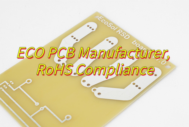
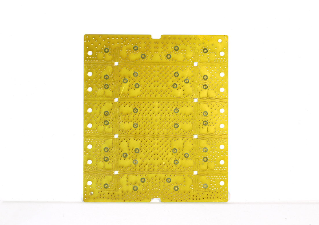
What Is ECO PCB?
ECO PCBs represent a sustainable evolution in circuit board technology, prioritizing environmental responsibility without compromising functionality. These boards eliminate hazardous substances like lead and halogenated flame retardants while incorporating recyclable materials and energy-efficient manufacturing processes.
The design focuses on reducing ecological impact through multiple approaches: using water-based cleaning systems, minimizing chemical waste, and enabling easier component recovery during recycling. Production methods emphasize lower energy consumption and reduced carbon emissions compared to conventional PCBs.
Compliant with international environmental standards such as RoHS and REACH, ECO PCBs serve industries requiring both technical performance and ecological accountability. Ongoing advancements explore biodegradable substrates and improved recycling techniques to further enhance sustainability. The technology demonstrates how electronics manufacturing can align with global environmental objectives while meeting modern technical demands.
Benefits of Eco-Friendly PCB
- Hazardous Substance Reduction: Eliminates toxins like halogens in materials.
- Recyclability: Metal cores and substrates reusable via smelting/shredding.
- Lower Carbon Footprint: Uses renewable/recycled resources instead of petroleum.
- Regulatory Compliance: Meets RoHS, REACH, and other global environmental standards.
- Waste Reduction: Biodegradable options cut landfill contributions.
- Safer Production: Non-toxic processes improve factory worker safety.
- Circular Economy Support: Materials designed for reuse in new products.
- Brand Value Boost: Appeals to eco-conscious consumers and investors.
- Resource Conservation: Reduces dependence on non-renewable materials.
- Future-Proofing: Aligns with emerging green tech regulations and trends.
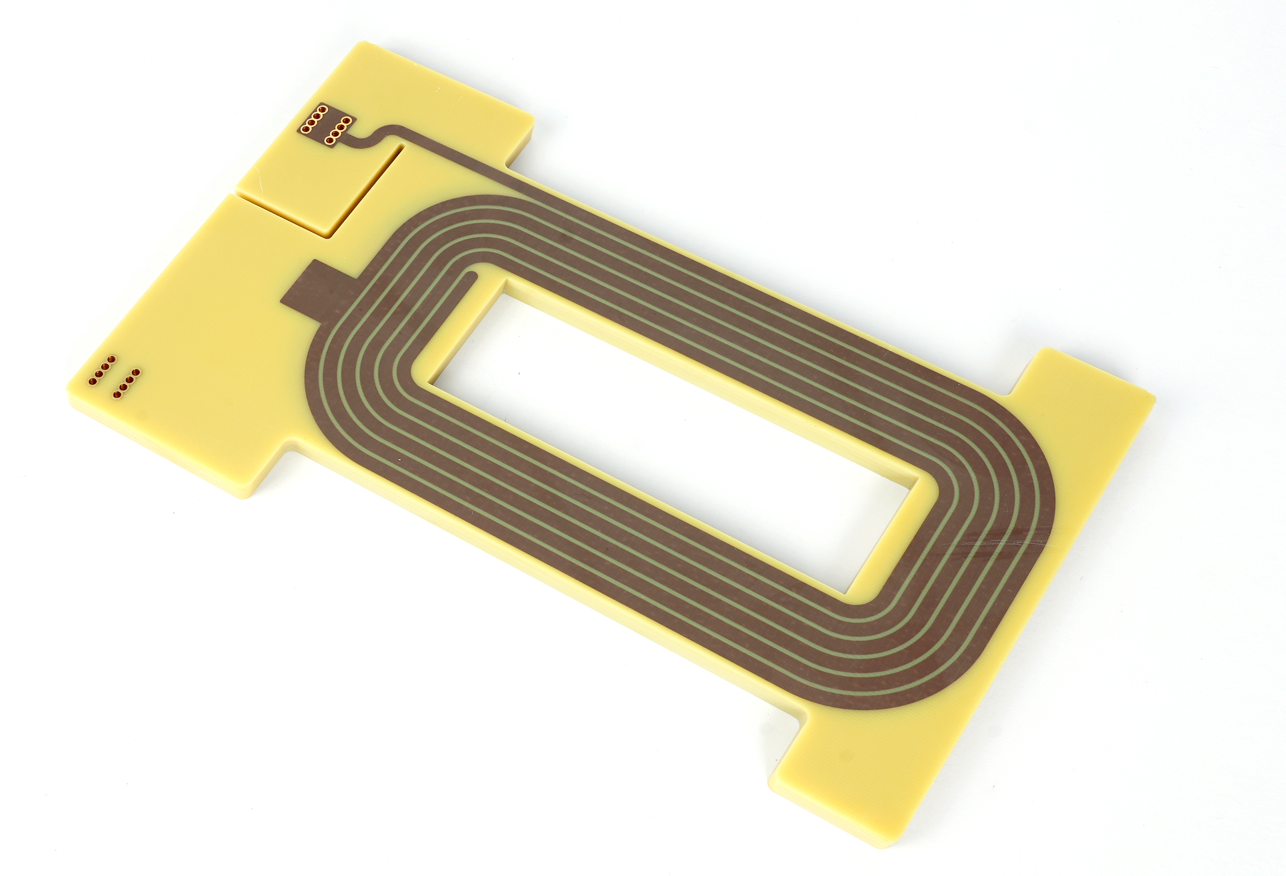
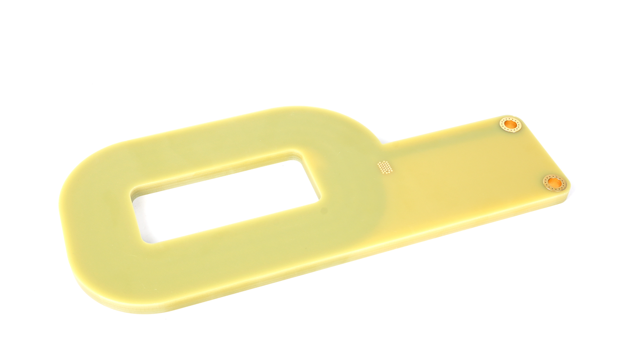
Application of ECO PCB
- Bio-Based Resins: Remote controls, environmental sensors.
- Recyclable Substrates: Street lighting LED drivers, electric vehicle battery modules.
- Halogen-Free Laminates: Portable medical ultrasound devices, factory motor controllers.
- Water-Soluble Solder Masks: Custom IoT sensor prototypes, wearable tech development.
- Low-Toxicity Metal Finishes: Satellite communication boards, drone flight control systems.
- Biodegradable Substrates: Short-term medical monitoring patches, perishable goods RFID tags.
Eco-Friendly PCB Material Innovations
Here are notable innovations in eco friendly PCB materials with practical applications:
Plant-Based Substrates
- Lignin-reinforced epoxy resins replacing 40% of petroleum content.
- Bamboo fiber composites for flexible circuits in wearables.
Recyclable Metal Layers
- Electrolytic copper foil with 99% recycling efficiency.
- Aluminum cores enabling full-board recovery in LED lighting.
Non-Toxic Bonding Agents
- Soy protein adhesives achieving 8N/mm peel strength.
- Chitosan-based dielectrics with 4.3 dielectric constant.
Bio-Degradable Carriers
- Polylactic acid (PLA) films for temporary circuit supports.
- Mycelium packaging replacing plastic trays in shipments.
Low-Energy Processing Materials
- UV-curable inks reducing curing energy by 65%.
- Room-temperature solder pastes melting at 138°C.
Advanced Flame Retardants
- Phosphorus-nitrogen compounds passing UL94 V-0.
- Silica aerogel coatings for high-voltage insulation.
ECO PCB Environmental Certification
- RoHS: Restricts hazardous substances (e.g., lead, mercury) in electrical/electronic products.
- REACH: Regulates chemical production, import, and use to protect human health/environment.
- UL ECVP: Validates environmental claims (e.g., recycled content, biodegradability).
- ISO 14001: Certifies environmental management systems for sustainable manufacturing.
- IEC 62321: Standardizes testing methods for restricted substances in electronics.
- TCO Certified: Ensures reduced environmental impact across product lifecycle (e.g., energy use, recyclability).
- EPEAT: Rates electronic products based on sustainability criteria (e.g., material selection, end-of-life management).
- Carbon Neutral Certified: Verifies net-zero carbon emissions through reduction/offsetting.
- Blue Angel: German ecolabel for low-pollution, resource-efficient products.
- Cradle to Cradle: Certifies materials for circularity (recyclable/biodegradable design).
ECO Friendly PCB Processes
- Water-Soluble Solder Masks: Enables easy component separation in IoT sensor prototypes.
- Bio-Based Resin Lamination: Reduces petroleum use in single-sided PCBs (e.g., remote controls).
- Low-Temperature Soldering: Cuts energy consumption by 40% in LED driver production.
- Closed-Loop Metal Recovery: Reuses copper/silver from waste in new PCB manufacturing.
- Halogen-Free Laminates: Meets REACH standards for portable medical devices (e.g., ultrasound units).
- UV-Curable Ink Printing: Lowers VOC emissions in flexible PCBs for wearable tech.
- Non-Cyanide Metal Plating: Uses silver coatings for automotive ADAS modules.
Future Trends in ECO Friendly PCB Development
Renewable Material Integration
- Plant-derived bio-resins replacing petroleum-based substrates.
- Recycled copper foil with ≥85% reclaimed content utilization.
Closed-Loop Processing
- Zero-discharge water recycling systems achieving >95% recovery rates.
- On-site metal reclamation from etching solutions via ion-exchange membranes.
Digital Manufacturing Ecosystems
- AI-driven resource optimization reducing material waste by 18-22%.
- Blockchain-enabled component traceability across supply chains.
Energetic Efficiency Breakthroughs
- Microwave-assisted lamination cutting energy consumption 40-50%.
- Photonic soldering replacing conventional reflow with 70% energy reduction.
Circular Design Frameworks
- Disassembly-optimized layouts enabling >90% component recovery.
- Transient electronics with programmable biodegradation timelines.
ECO Friendly PCB Manufacturer with RoHS Compliance – EBest Circuit (Best Technology)
Reasons why choose EBest Circuit (Best Technology) as your ECO PCB manufacturer:
Certified Environmental Compliance
- Full RoHS/REACH certification (Pb/Cd/Hg/Cr⁶⁺/PBB/PBDE-free).
- Halogen-free materials (Br/Cl <900ppm per IEC 61249-2-21).
Advanced Green Processes
- Lead-free HASL and immersion gold finishes.
- Closed-loop water recycling (95%+ recovery rate).
- VOC-free cleaning with biodegradable saponifiers.
Rapid Turnkey Services
- 24-hour prototype delivery for urgent designs.
- Standard 3-5 day production cycles for bulk orders.
- Real-time DFM feedback within 2 hours.
Transparent cost structure
- Standardized quotation system (no hidden fees)
- Scale procurement reduces costs by 15-20%
Rigorous Quality Control
- ISO 9001:2015 & IATF 16949 certified
- 100% electrical testing + AOI/AXI inspection
- IPC Class 2/3 reliability standards
Technical Support
- Free engineering consultations for DFM/DFA
- Dedicated account managers for ECO updates
- Lifetime traceability via blockchain records
If you have any request for eco-friendly PCB, welcome to contact EBest Circuit (Best Technology): sales@bestpcbs.com. Looking forward to hearing from you soon!
You may also like
Tags: eco friendly pcb, eco pcb