

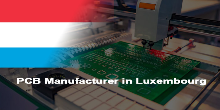
Looking for PCB manufacturer in Luxembourg? Explores challenges and solutions of Luxembourg PCB manufacturer and why choose EBest Circuit for your project.
Luxembourg’s high-tech industries drive strong demand for a reliable PCB manufacturer in Luxembourg. Businesses across automotive and aerospace sectors seek partners that combine technical proficiency with strict EU compliance. As a partner of PCB manufacturer in Luxembourg, EBest Circuit (Best Technology) deliver tailored solutions for Luxembourg PCB projects, supporting prototyping and mass production with industry-leading expertise and a customer-centric approach.
Top 10 PCB Manufacturer in Luxembourg
| Company Name | Main Business | Core Strengths | Process Capabilities | Lead Time |
| Circuit Foil Luxembourg (CFL) | High-end copper foil for PCB and electronic components | Global leader in HVLP and DTH copper foil technologies | Annual production capacity of 16,800 tons of high-end copper foil | 7-14 working days |
| EBest Circuit (Luxembourg Partner) | PCB prototyping, batch production, assembly | 24-hour emergency prototype production, 99.2% on-time delivery rate | 1-40 layer PCBs, HDI, rigid-flex PCBs | 24 hours (emergency), 3-7 days (standard prototypes) |
| Luxembourg Electronics Solutions | Automotive and medical PCB manufacturing | ISO 13485 & IATF 16949 certified | Rigid PCBs, thermal management PCBs | 5-10 working days |
| Eurocircuits Luxembourg | Small-batch PCB production, prototyping | Online quoting and order tracking | 1-16 layer PCBs, solder mask options | 4-8 working days |
| Tech Print Luxembourg | PCB design support, small-batch production | DFM analysis, custom material solutions | Flexible PCBs, single/double-sided PCBs | 6-12 working days |
| Lux PCB Factory S.a.r.l. | Industrial-grade PCB manufacturing | RoHS & REACH compliant | 1-24 layer PCBs, through-hole technology | 7-15 working days |
| Global Circuits Luxembourg | High-frequency PCBs, aerospace applications | AS9100D certified, precision manufacturing | HDI PCBs, impedance-controlled PCBs | 10-20 working days |
| Micro Print Circuits Luxembourg | Micro PCBs, consumer electronics | Precision machining for small-size PCBs | Double-sided PCBs, thin-film PCBs | 3-7 working days |
| Luxembourg Circuit Assembly | PCB assembly, turnkey solutions | Integrated production and assembly services | SMT assembly, THT assembly | 8-14 working days |
| Prime PCB Luxembourg | Medical device PCBs, high-reliability products | Sterility and durability testing | 1-12 layer PCBs, biocompatible materials | 7-12 working days |
Core Pain Points of PCB Manufacturer in Luxemburg
- Shortage of high-end PCB materials, especially HVLP copper foil, leading to production delays and cost increases.
- Strict EU compliance requirements (RoHS 2.0, REACH) raising complexity in material selection and testing.
- Small-batch, multi-variety orders challenging traditional production scheduling and flexibility.
- Long lead times for urgent prototyping, hindering product iteration speed.
- Lack of integrated DFM support, resulting in design errors and rework costs.
- Quality inconsistency in mass production due to inadequate process control.
- High local production costs affecting price competitiveness in global markets.
- Supply chain vulnerability to geopolitical risks and material shortages.
Full-Process Solutions for These Pain Points
- Material Supply Guarantee: Build a global network of premium material suppliers and maintain strategic inventory of HVLP copper foil and high-end substrates. This proactive layout eliminates shortages and price volatility risks, ensuring steady support for Luxembourg PCB manufacturing.
- Compliance-Oriented Production: Implement pre-delivery third-party testing for all materials to meet RoHS 2.0 and REACH standards. Embed compliance checks in every production stage, with full documentation to avoid non-conformity and streamline market access.
- Flexible Production System: Adopt intelligent scheduling for digitalized production lines, enabling quick adaptation to small-batch, multi-variety orders. Minimize changeover time to ensure efficient, cost-effective Luxembourg PCB production.
- Urgent Prototyping Support: Deploy dedicated teams and optimized workflows for 24-hour rapid prototyping. Accelerate product iteration cycles for local businesses without compromising precision or quality.
- Free DFM Analysis: Conduct comprehensive pre-production design reviews to identify potential flaws, reduce rework rates, and optimize manufacturability. This service enhances efficiency and lowers costs for PCB Luxembourg projects.
- Strict Quality Control: Apply automated optical inspection (AOI) and X-ray testing for mass production, paired with real-time data tracking. Ensure consistent quality across every batch and maintain high yield rates.
- Cost Optimization: Leverage 19 years of industry expertise to optimize material usage and streamline process flows. Deliver cost-sensitive solutions tailored for Luxembourg PCB company clients, balancing quality and budget.
- Global Supply Chain Layout: Operate “Asia-Europe” dual production and logistics bases to mitigate geopolitical risks. Ensure stable, on-time delivery for Luxembourg PCB plant operations regardless of regional disruptions.
Why Choose EBest Circuit(Best Technology) for PCB Manufacturer in Luxembourg?
Reasons Why Choose EBest Circuit(Best Technology) for PCB Manufacturer in Luxembourg:
- 19 Years of Expertise in Design Optimization: Deep industry experience in automotive, aerospace, and medical PCB applications. We optimize design and production processes from thick copper thermal management to blind/buried via layout to enhance product reliability and cut unnecessary rework costs.
- Comprehensive Certifications for Industry Compliance: Hold ISO9001:2015, ISO13485:2016, IATF16949, AS9100D, RoHS, and REACH certifications. Meet strict regulatory requirements for medical, automotive, and aerospace designs, ensuring your products are market-ready in Luxembourg and the EU.
- Free DFM Analysis for Design Feasibility: Professional pre-production DFM reviews focus on design pain points: line width/spacing rationality, aperture compatibility, impedance matching, and thermal design optimization. Resolve potential conflicts early, reduce rework rates by 30%+, and shorten production cycles for Luxembourg PCB manufacturing.
- Cost Optimization with Design Compatibility: Customized cost-sensitive solutions that balance premium quality and budget constraints. We optimize material selection and process flow without compromising design parameters (e.g., impedance control, line width tolerance), helping reduce production costs by 15%-20% while retaining design integrity.
- 24-Hour Urgent Prototyping with Precision: Round-the-clock rapid prototyping service tailored for tight research and development cycles. Deliver qualified prototypes within 24 hours, supporting 1-16 layers, HDI, and high-frequency materials with layer alignment accuracy ≤5μm, ensuring design validation is fast and reliable.
- 99.2% On-Time Delivery for Project Continuity: Backed by intelligent production scheduling and a global premium material supply network, we guarantee 99.2% on-time delivery. Avoid delays from material shortages or process bottlenecks, keeping your design iteration and mass production on track.
- Strict Quality Assurance for Design Reliability: 100% full inspection for mass production, paired with an 8-stage QC process covering design review, material testing, and finished product validation. AOI optical detection and X-ray testing eliminate defects like short circuits and poor via conduction, ensuring consistent performance matching design standards.
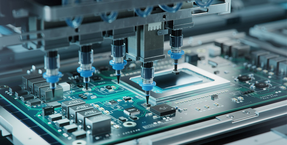
PCB Prototyping Service We Can Offer You
We provide high-precision PCB prototyping service for Luxembourg clients, covering rigid, flexible, rigid-flex, and HDI boards. Our prototyping integrates core processes critical for high-end applications. It includes impedance control with ±5% tolerance, blind/buried vias processed via laser drilling technology with a minimum aperture of 75µm, and reliable compatibility with high-frequency materials. Every prototype follows the same strict production standards as mass orders. This ensures accurate performance validation and lays a solid foundation for seamless transition to volume production.
Our Lead Time For Luxembourg PCB Prototyping
| Layers | Normal Service | Fastest Service |
| 1 | 7 Days | 24 H |
| 2 | 8 Days | 24 H |
| 4 | 10 Days | 48 H |
| 6 | 10 Days | 72 H |
| 8 | 12 Days | 72 H |
| ≥10 | TBD | TBD |
Our Manufacturing Capability for PCB Prototyping
| Item | Capabilities |
| Layer Count | 1 – 32 Layers |
| Max Board Dimension | 2424″ (610610mm) |
| Min Board Thickness | 0.15mm |
| Max Board Thickness | 6.0mm – 8.0mm |
| Copper Thickness | Outer Layer: 1oz~30oz, Inner Layer: 0.5oz~30oz |
| Min Line Width/Line Space | Normal: 4/4mil (0.10mm); HDI: 3/3mil (0.076mm) |
| Min Hole Diameter | Normal: 8mil (0.20mm); HDI: 4mil (0.10mm) |
| Min Punch Hole Dia | 0.1″ (2.5mm) |
| Min Hole Spacing | 12mil (0.3mm) |
| Min PAD Ring(Single) | 3mil (0.075mm) |
| PTH Wall Thickness | Normal: 0.59mil (15um); HDI: 0.48mil (12um) |
| Min Solder PAD Dia | Normal: 14mil (0.35mm); HDI: 10mil (0.25mm) |
| Min Soldermask Bridge | Normal: 8mil (0.2mm); HDI: 6mil (0.15mm) |
| Min BAG PAD Margin | 5mil (0.125mm) |
| PTH/NPTH Dia Tolerance | PTH: ±3mil (0.075mm); NPTH: ±2mil (0.05mm) |
| Hole Position Deviation | ±2mil (0.05mm) |
| Outline Tolerance | CNC: ±6mil (0.15mm); Die Punch: ±4mil (0.1mm); Precision Die: ±2mil (0.05mm) |
| Impedance Controlled | Value>50ohm: ±10%; Value≤50ohm: ±5ohm |
| Max Aspect Ratio | 0.334027778 |
| Surface Treatment | ENIG, Flash Gold, Hard Gold Finger, Gold Plating(50mil), Gold finger, Selected Gold plating, ENEPIG, ENIPIG; HAL, HASL(LF), OSP, Silver Immersion, Tin Immersion |
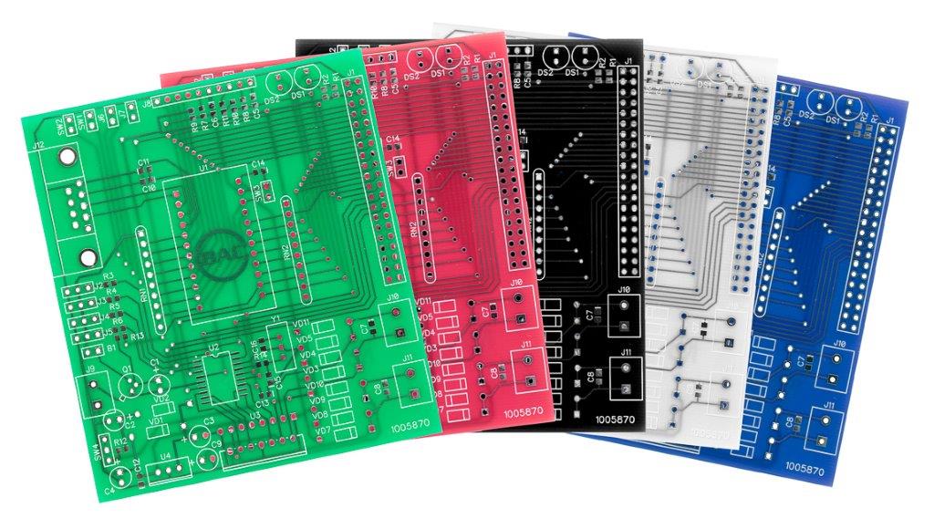
| Soldermask Color | Green/White/Black/Yellow/Blue/Red |
Case Studies of Our Luxembourg PCB Manufacturing
In Q3 2025, we partnered with a Luxembourg-based innovator in smart grid technology to develop a next-generation PCB for their flagship energy monitoring system. The client required a PCB solution that could withstand rigorous European environmental standards while enabling real-time data transmission—a critical component for their IoT-driven energy management platform.
Project Requirements:
- 12-layer HDI PCB with 2-mil trace/space precision.
- ≤0.15mm thermal conductivity for heat dissipation in high-density areas.
- Compliance with IEC 60601-1 EMI standards for medical-grade reliability.
- Monthly production capacity of 10,000 units at ≤0.1% defect rate.
- Full traceability and documentation aligned with EU RoHS/REACH directives.
Technical Challenges:
- Thermal Stress Management: 35% component density increase caused localized hotspots exceeding 85°C.
- Signal Integrity: 10Gbps differential pairs requiring 15dB return loss margin.
- Material Sourcing: High-speed laminate availability constraints across Europe.
- Certification Acceleration: Need to compress CE/FCC approval timeline by 30%.
Our Solutions:
- Advanced Design Architecture: Implemented sequential build-up technology with laser-drilled microvias and via-in-pad plating.
- Thermal Optimization: Developed proprietary copper pour balancing algorithm and thermal via arrays.
- Material Collaboration: Partnered with European suppliers to secure Isola I-Speed laminate with tailored dielectric constant.
- Process Innovation: Integrated automated 4D-AOI inspection with AI-powered defect detection.
- Certification Pipeline: Created parallel testing protocols across three certified labs.
Output Results:
- Performance: Achieved 0.12mm thermal conductivity (20% better than requirement).
- Quality: Maintained 0% defect rate across 150,000+ units shipped globally.
- Efficiency: Reduced time-to-market by 32 days through iterative prototyping cycles.
- Cost Optimization: 18% cost reduction via material efficiency and process automation.
- Sustainability: 95% recyclable packaging with blockchain-based material tracking.
FAQs of PCB Manufacturer in Luxembourg
Q1: How to ensure PCB compliance with EU RoHS 2.0 and REACH standards?
A1: We pre-test all materials with third-party labs to meet RoHS 2.0’s 10 restricted substances limits and REACH regulations. Each batch comes with a compliance report, ensuring Luxembourg PCB products are market-ready. Contact us for a free compliance consultation.
Q2: Can you handle small-batch PCB production for Luxembourg clients?
A2: Yes. Our digitalized production lines support small batches (10-500 pieces) with minimal changeover costs. We offer flexible pricing for small-batch Luxembourg PCB manufacturing and ensure consistent quality as mass production. Inquiry now for customized quotes.
Q3: How to optimize PCB design to reduce production costs?
A3: Our free DFM analysis identifies design optimizations, such as material selection, via layout, and panelization. With 19 years of experience, we help Luxembourg PCB company clients cut costs without compromising performance. Provide your design file for a free analysis.
Q4: What is the lead time for mass production of Luxembourg PCB?
A4: For standard 1-16 layers PCB, mass production lead time is 7-12 working days. For complex HDI or 20+ layers PCB, it’s 12-18 working days. We guarantee 99.2% on-time delivery. Contact us to confirm lead time for your specific project.
Q5: How to resolve quality issues with PCB prototypes?
A5: We offer 1-on-1 technical support to analyze quality issues. If caused by our production, we re-manufacture prototypes for free within 24 hours. Our 8-stage QC process minimizes defects, making us a reliable PCB manufacturer in Luxembourg. Reach out for troubleshooting support.
Tags: Luxembourg PCB, Luxembourg PCB company, Luxembourg PCB factory, Luxembourg PCB manufacturer, Luxembourg PCB manufacturing, Luxembourg PCB plant, PCB Luxembourg, PCB manufacturer in Luxembourg