

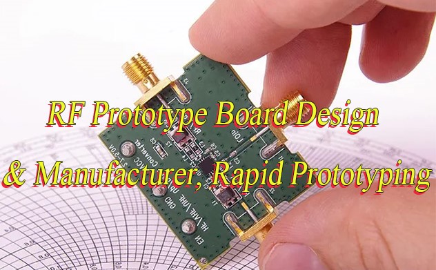
Why do RF Prototype board? Let’s discover benefits, applications, design technical spec, production process, cost and lead time for RF board prototype.
Are you worried about these problems?
- Is design validation stuck in endless iterations?
- Are small-batch prototypes too costly?
- Can urgent orders meet deadlines?
As a RF prototype board manufacturer, EBest Circuit (Best Technology) can provide you service and solutions:
- 24-Hour Rapid Prototyping: Dedicated line for urgent needs, sample delivery within 24 hours. Cuts validation time by 60%, accelerates time-to-market.
- Cost-Optimized Design Guidance: Leverage 5000+ case database and free DFM analysis. Optimizes material selection, routing, and process steps to reduce small-batch costs by 15–30% without compromising quality.
- Full-Batch Inspection & Traceable Quality: ISO 19001-certified process with 100% batch inspection. Combines systematic visual checks and manual verification, maintaining 99.2%+ yield and <3% rework rate. Each board’s quality is fully traceable.
Welcome to contact us if you have any request for RF PCB design, prototyping, mass production, assembly: sales@bestpcbs.com.
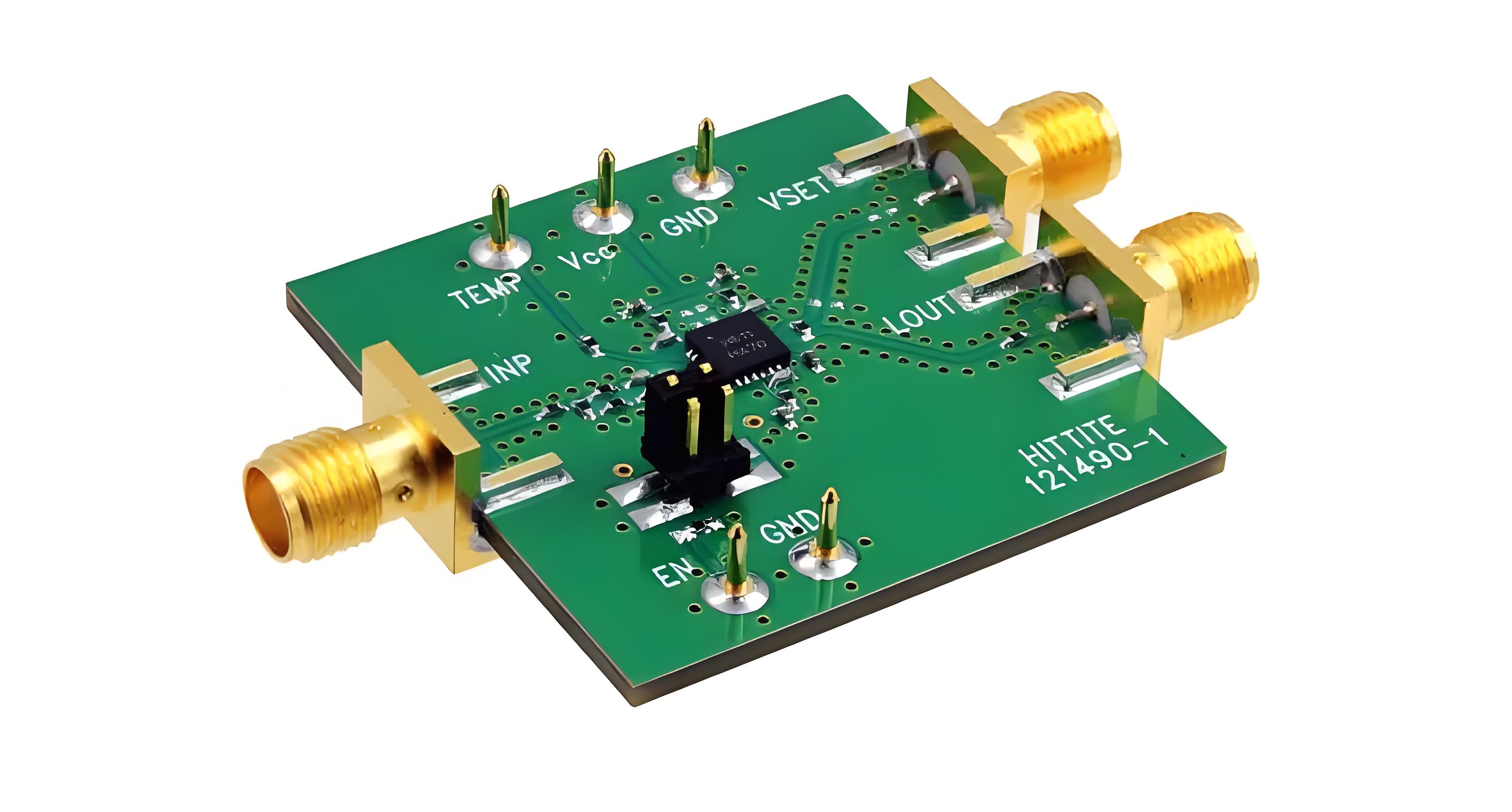
What Is A RF Prototype Board?
A RF Prototype Board is an initial physical circuit board created specifically for testing and validating RF circuit designs. As a physical sample during the design phase, it is used to actually measure RF performance characteristics (such as impedance matching, signal integrity, gain, and noise), verify the feasibility of high-frequency board material selection, layout, routing, and functionality, and provide a reliable basis for subsequent design iterations or mass production. Its core value lies in quickly exposing design problems at a controllable cost, ensuring that the final product meets stringent RF performance requirements.
Why Do RF Board Prototype?
Advantages of RF board prototype:
- Verify Design Feasibility and Save Costs: RF circuits are highly sensitive to high-frequency signal paths and impedance matching. Prototyping quickly validates whether physical parameters like microstrip line width and via placement meet 50Ω impedance requirements, preventing mass production failures that could cost tens of thousands of dollars in rework expenses.
- Ensure Performance Compliance: Prototyping enables real-world testing of critical metrics (e.g., S-parameters, phase noise). By analyzing S11/S21 via vector network analyzers, engineers can pinpoint impedance mismatch issues and adjust component values (capacitors/inductors) to meet specifications like -100dBm receive sensitivity or +30dBm output power, enhancing device range and stability.
- Address EMI and Thermal Challenges Early: Prototypes allow early detection of electromagnetic interference (EMI) hotspots through near-field scanning and thermal issues via infrared imaging. This facilitates rapid optimization of ground plane segmentation, shielding structures, or heat dissipation designs—reducing time and budget by over 50% compared to post-production modifications.
- Accelerate Iteration and Align with Customer Needs: Physical prototypes serve as tangible validation tools for client demos or field testing. For example, in 5G small cell development, prototypes integrated into customer systems enable real-time feedback on coverage and data rates. This iterative process (3–5 cycles) ensures design alignment with market requirements, cutting time-to-market by 30% or more.
- Meet Regulatory and Industry Standards: Prototyping facilitates pre-compliance testing for certifications like FCC/CE. By verifying adherence to standards (e.g., EN 300 328 for 2.4GHz devices or 47 CFR Part 15), designers can proactively adjust parameters (filter cutoff frequencies, shield dimensions) to ensure first-pass certification success, avoiding delays in product launch.
When to Use RF Prototype Board?
Applications of RF prototype board:
- First-Version Verification of New RF Architectures: When implementing complex designs for the first time (e.g., millimeter-wave arrays or multi-stage LNA chains), real-world measurement of nonlinear effects and inter-stage interference is mandatory, as simulation cannot fully replicate these phenomena.
- Evaluation of High-Frequency Material Transitions: When switching substrate suppliers (e.g., Rogers to Tachyon) or adopting cost-effective alternatives, prototype boards are required to quantify differences in insertion loss and phase stability.
- On-Site Antenna System Matching: When antenna impedance is influenced by mechanical components or human-machine interactions, prototypes enable real-environment debugging of matching networks (e.g., compensating for 5G antenna frequency shifts caused by smartphone chassis).
- Pre-Certification EMC Risk Mitigation: Prior to FCC/CE submission, prototypes are used for self-testing radiation spectra to identify issues like clock harmonics or switching noise coupling, preventing certification failures that delay projects.
- Production Process Limit Testing: When evaluating risky processes such as low-cost FR4 hybrid high-frequency materials or ultra-fine-pitch BGA soldering, prototypes validate mass production feasibility (e.g., tolerance of 77GHz microstrip lines in automotive radar).
- Multi-Board System Integration Debugging: When integrating RF subsystems (e.g., FEM + transceiver chips) with digital boards, prototypes expose cross-board ground bounce and crosstalk issues often overlooked in simulation models due to connector parasitics.
- Customer Acceptance Prototype Delivery: For customers requiring advance validation of hardware metrics (e.g., contractual PA efficiency requirements for base station OEMs), prototype boards serve as the sole legally binding deliverable.
RF Prototyping Board Design Technical Requirements
| Technical Parameter | Typical Requirement |
| Operating Frequency Range | DC-40 GHz (Millimeter-Wave Extended to 80 GHz) |
| Single-Ended Impedance Tolerance | ±5% (Strict Scenarios ±3%) |
| Differential Impedance Tolerance | ±7% |
| Dielectric Constant (Dk) Tolerance | ±0.2 (e.g., Rogers 4350B@10GHz) |
| Loss Tangent (Df) | ≤0.003@10GHz |
| Line Width/Spacing Tolerance | ±0.02mm (High-Speed Board) / ±0.05mm (Conventional) |
| Interlayer Alignment Error | ≤0.075mm |
| Back-drilled Stub Length | ≤0.1mm (>5GHz Required) |
| Hole Wall Roughness (Ra) | ≤1.5μm |
| Copper Foil Type and Roughness | RTF/VLP Copper Foil (Rz≤2μm) |
| Immersion Gold Thickness | 0.05-0.2μm (ENIG Process) |
| Material Thermal Conductivity | ≥0.6 W/mK (e.g., Rogers TMM Series) |
| Multi-Channel Phase Consistency | ±2°@Target Frequency |
| S21 Insertion Loss Variation | ≤±0.3dB/inch (@40GHz) |
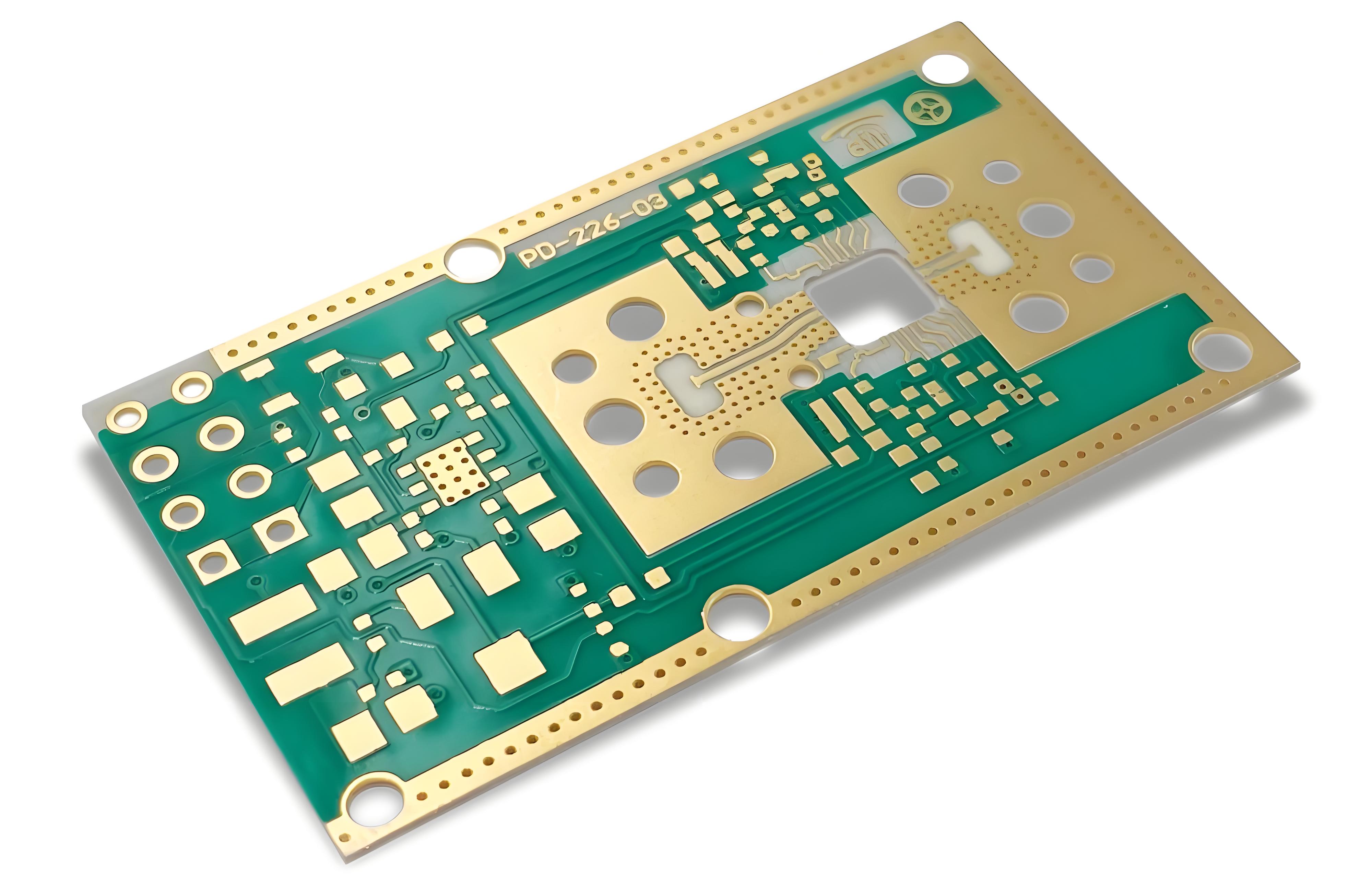
RF Circuit Board Prototyping Process
1. Material Selection: Choose low dielectric constant (Dk) and low loss (Df) substrates (e.g., Rogers RO4000, PTFE ceramic composites). Use reversed copper foil to reduce high-frequency skin effect.
2. Panel Cutting: Cut 1020mm×1020mm copper-clad laminates to design dimensions, optimizing panel size to improve material utilization (e.g., n-division cutting of raw materials) and reduce waste edge costs.
3. Drilling and Hole Metallization: Perform high-precision CNC drilling for through-holes/blind holes with hole diameter tolerance ≤±0.1mil. PTFE materials require plasma desmear treatment. Use chemical copper plating + electroplating thickening to ensure hole wall copper thickness ≥20μm for interlayer electrical connectivity.
4. Imaging and Etching: Adopt LDI (Laser Direct Imaging) technology to precisely replicate circuit patterns via high-energy UV laser scanning of photoresist dry film, achieving line width tolerance ±0.1mil. Remove non-circuit copper with acidic/alkaline etching solutions, combined with side-etch control to maintain impedance consistency (deviation ≤±5%). Validate via AOI/AVI for line width deviation and copper residue defects.
5. Lamination and Pressing: For multilayer boards, use symmetric stack-up structures (e.g., 3+3 layers) pressed at 180℃/300PSI to prevent warpage. High-layer-count boards employ stepped pressing for staged stacking to ensure uniform interlayer bonding. After outer layer circuit completion, apply solder mask (green oil) printing and silkscreen marking, forming protective layers via exposure and development.
6. Surface Finish and Profiling: Surface finishes include ENIG, HASL (Hot Air Solder Leveling), OSP, etc. Gold fingers are plated with hard gold for wear resistance. Use CNC routing/V-scoring for precise board separation, with rounded corners/edge grinding for smooth edges.
7. Electrical Performance Testing: Conduct flying probe tests/test fixtures to detect open/short defects. Use four-wire low-resistance testing for precise low-resistance measurement. Validate impedance consistency (deviation ≤±10%) via TDR (Time Domain Reflectometry) and measure S-parameters (insertion loss, return loss) with VNA (Vector Network Analyzer) to ensure RF performance compliance.
8. Environmental Reliability Testing: Verify material stability through thermal cycling tests and assess extreme environment adaptability via thermal shock tests. Use microsection inspection to check hole wall copper thickness and interlayer alignment accuracy (error ≤5μm), ensuring no delamination or warpage defects.
9. Visual and Functional Inspection: Identify circuit defects via AOI (Automated Optical Inspection) and assist manual inspection with AVI (Automated Visual Inspection) systems. Conduct FQA (Final Quality Audit) to ensure flawless appearance. Perform 100% electrical testing across all test points to eliminate functional defect leakage.
10. Sample Delivery and Validation: Execute final inspection before delivery, with ESD (Electrostatic Discharge)-compliant packaging and attached test reports/process specifications. Customers conduct soldering tests and signal integrity validation post-receipt, providing feedback for design iterations (e.g., trace width adjustment, layout optimization).
How Long Does A RF PCB Prototype Take?
| Layer Count | Standard Prototyping Time | Expedited Service Options |
| Double-sided RF PCB | 3–5 days | 24 hours |
| 4-layers RF PCB | 5–8 days | 48 hours |
| 6–8-layers RF PCB | 10–15 days | 96 hours |
How Much Does a RF PCB Prototype Cost?
| Layer Count | Substrate Type | Engineering Fee | Manufacturing Cost | Estimated Total (10 pcs) |
| Double-sided RF PCB | Rogers RO4000 Series | $70–$150 | $180–$450 | $250–$600 |
| 4-layers RF PCB | Hybrid (FR4 + High-Frequency) | $120–$300 | $300–$800 | $420–$1,100 |
| 6–8 layers RF PCB | High-Frequency Multilayer Lamination | $250–$600 | $800–$2,000 | $1,050–$2,600 |
Why Choose EBest Circuit (Best Technology) as RF Prototype Board Manufacturer?
Reasons why choose us as RF prototype board manufacturer:
- Extreme Cost-Sensitive Solutions: Offer industry-leading price competitiveness with customized cost-optimization designs, directly reducing clients’ RF prototype development budgets. Ideal for cost-sensitive innovation projects, achieving a win-win of high performance and low investment.
- 24-Hour Rapid Prototyping for Urgent Orders: Address needs during critical R&D phases with a commitment to complete urgent orders within 24 hours, significantly shortening product validation cycles and accelerating market entry by over 40%.
- 99.2% On-Time Delivery Rate: Leverage intelligent supply chain management to achieve a 99.2% on-time delivery rate, far exceeding industry averages. Ensures client project timelines remain on track, avoiding delays and associated costs.
- Authoritative Certification Backing: Hold certifications including ISO 19001, IATF 16949, medical-grade standards, and RoHS compliance. Covers high-demand sectors from consumer electronics to medical and automotive, enabling clients to leverage shared certifications for faster regulatory approval.
- 19 Years of Industry Expertise: With 19 years focused on RF prototype board manufacturing, accumulate over 5,000 case studies and a proprietary production error database. Proactively optimize designs using historical data to help clients avoid common defects and reduce rework costs by 30%.
- Free DFM Design Optimization: Provide expert free DFM (Design for Manufacturability) analysis, guiding material selection, process paths, and wiring optimization. Identify design risks early to reduce modification costs and boost first-pass success rates to 98%.
- Agile Production Capacity: Equip multiple smart production lines to support seamless transitions from small-batch prototypes to volume production. Quickly adjust capacity to meet full lifecycle needs from R&D to market launch, avoiding wasted resources.
- 24/7 Dedicated Technical Support: Offer round-the-clock technical response with a senior engineer team providing one-on-one support. Ensure client issues are addressed within 8 hours and solutions provided within 48 hours, safeguarding project success throughout.
Our Lead Time for RF Board Prototype
| Layers | Normal Service | Fastest Service |
| 1 | 7 Days | 24 H |
| 2 | 8 Days | 24 H |
| 4 | 10 Days | 48 H |
| 6 | 10 Days | 72 H |
| 8 | 12 Days | 72 H |
| ≥10 | TBD | TBD |
How to Get a Quote for RF Board Prototyping?
List of materials required for RF PCB prototyping:
- Gerber Files: Complete PCB design files including circuit layers, solder mask layers, and silkscreen layers (must specify version and design software information, e.g., Altium Designer 24.x format).
- BOM (Bill of Materials): Detailed list of all electronic components with model numbers, brands, package specifications, and quantities (must include key parameters for RF components such as resistance/capacitance values and transistor specifications).
- Stack-Up Specifications: Clear description of substrate types for each layer (e.g., Rogers RO4003C), copper foil thickness (e.g., 1/2 oz reversed copper foil), dielectric layer thickness, and layer stacking sequence (e.g., L1 signal layer/L2 ground layer/L3 power layer).
- Impedance Control Requirements: Specified impedance values and tolerance ranges (±5%~±10%) for RF paths (e.g., 50Ω microstrip lines, striplines), with annotated trace width/spacing parameters for matching.
- Surface Finish Selection: Explicitly state surface finish process type (e.g., ENIG, OSP, immersion silver), with special annotations for gold finger plating thickness and wear resistance requirements.
- Special Process Requirements: For processes such as blind/buried vias, back drilling, via-in-pad plugging, or electroplated fill holes, provide specific hole size ranges (≥0.2mm) and position annotations.
- Test Verification Requirements: Include electrical performance tests (e.g., flying probe test, four-wire low-resistance test), RF parameter tests (S-parameters, insertion loss), and environmental reliability tests (thermal cycling, thermal shock).
- Quantity and Lead Time: Specify prototype quantity (e.g., 5-10 pieces), standard lead time requirements (e.g., 5-8 days), and expedited service options.
Welcome to contact us if you have any request for RF board prototyping: sales@bestpcbs.com.