

PWB vs PCB are two acronyms frequently encountered in electronics manufacturing, both referring to the foundational platforms for mounting and connecting electronic components. This article will delve into the nuances: PCB vs PWB, explore their applications, and help you determine which is better suited for your modern electronic projects.
Are you struggling to select the right type of board for your electronic application, often facing challenges related to terminology, design complexity, and performance requirements? Many engineers and procurement specialists encounter similar hurdles.
- Confusion over the exact difference between PWB and PCB and whether the distinction impacts sourcing.
- Difficulty in selecting the appropriate board type (PWB board vs. a more complex PCB) for a specific project’s cost and functionality needs.
- Encountering reliability issues, such as short circuits or signal integrity problems, with substandard boards.
- Challenges in managing the PWB assembly or PCBA process, especially for complex, multi-layer designs.
- Navigating the procurement process without a reliable supplier who can provide expert guidance and high-quality manufacturing.
These challenges can be effectively addressed by partnering with an experienced manufacturer who clarifies these terms and delivers robust solutions.
- Expert clarification on PWB vs PCB wiring and terminology, ensuring you specify the correct product for your PWB electronics application.
- Guidance on material selection and board type—whether a simple printed wiring board or a high-density interconnect (HDI) PCB—to optimize performance and cost.
- Utilization of high-quality materials and stringent quality control processes to ensure board reliability and longevity.
- Comprehensive services that cover everything from design support to full PWB assembly and testing, simplifying your supply chain.
- Access to a trusted partner like BEST Technology, a professional PCB manufacturer with a proven track record in producing high-reliability boards for diverse industries.
At BEST Technology, we specialize in the manufacturing of advanced printed circuit boards, including both PWBs and PCBs. With two decades of experience, state-of-the-art facilities, and a commitment to quality, we help our clients navigate the complexities of electronic board selection and production. For inquiries, please contact us at sales@bestpcbs.com.
What does PWB Stand for?
PWB stands for Printed Wiring Board. This term historically refers to a bare board that provides the mechanical support and electrical connections for components using conductive tracks, pads, and other features etched from copper sheets laminated onto a non-conductive substrate. In essence, it is the foundational structure for “wiring” components together.
- Historical Context: The term PWB was more commonly used in the early days of the electronics industry, particularly in certain regions like Japan. It emphasizes the board’s primary function as an interconnect platform before the widespread integration of active and passive components directly onto the board itself.
- Modern Interpretation: Today, PWB is often used interchangeably with PCB, though a subtle distinction persists in some technical circles, which we will explore later.
In summary, PWB denotes the basic board that forms the electrical wiring backbone of an electronic assembly.
What are the Different Types of PWBs?
PWBs can be categorized based on their construction and the number of conductive copper layers they possess. The primary types are:
- Single-Sided PWBs: These boards have a conductive copper layer on only one side of the substrate.
Components are placed on one side, and the circuitry is etched on the other.
They are the simplest and most cost-effective type, suitable for basic electronic devices. - Double-Sided PWBs: These feature conductive layers on both sides of the substrate.
The two sides are connected using plating through holes (PTHs), allowing for more complex circuits and higher component density than single-sided boards. - Multi-Layer PWBs: These consist of three or more layers of conductive material, separated by insulating layers (prepreg) and laminated together.
They are used in highly complex electronics like smartphones, computers, and medical equipment, where high circuit density and signal integrity are paramount.
In conclusion, the type of PWB—single-sided, double-sided, or multi-layer—is chosen based on the complexity, size, and performance requirements of the electronic device.
What Materials are Used in PWBs?
The performance, cost, and application of a PWB are largely determined by the materials used in its construction. The key materials include:
- Substrate (Laminate): This is the insulating base material.
The most common is FR-4, a glass-reinforced epoxy laminate known for its good mechanical strength and flame retardancy.
For high-frequency applications, materials like PTFE (Teflon) or ceramic-filled hydrocarbons are used. - Copper Foil: This conductive layer is laminated onto the substrate.
It is etched to form the circuit traces.
The thickness of the copper is typically measured in ounces per square foot (e.g., 1 oz, 2 oz). - Solder Mask: This polymer layer is applied over the copper traces to prevent solder bridges between closely spaced pads during assembly and to protect the copper from oxidation and environmental damage.
It is typically green, but other colors are available. - Silkscreen: This is the layer where letters, numbers, and symbols are printed on the board to assist in component placement and identification.
The careful selection of these materials is crucial for ensuring the electrical PCB performs reliably under its intended operating conditions.
How do you Design a PWB?
Designing a PWB is a critical, multi-step process that translates a circuit schematic into a physical board layout ready for manufacturing.
- Schematic Capture: The process begins with creating a schematic diagram using Electronic Design Automation (EDA) software. This diagram represents the electrical connections between components.
- Component Placement: The physical components from the schematic are placed on the board layout within the EDA software. Optimal placement is key for signal integrity, thermal management, and manufacturability.
- Routing: This involves drawing the copper traces that will connect the components according to the schematic. Design rules (e.g., trace width, spacing) must be strictly followed.
- Design Rule Check (DRC): The software automatically checks the layout against a set of predefined rules to identify errors like short circuits or insufficient clearances.
- Gerber File Generation: Once the design is error-free, a set of files (Gerbers) is generated. These files contain all the necessary information for manufacturing, including copper layers, solder mask, and silkscreen.
A well-executed PWB design is fundamental to the functionality and reliability of the final electronic product.
What are the Advantages of Using PWBs?
PWBs offer several significant advantages over older point-to-point wiring methods, making them indispensable in modern electronics.
- Reliability and Repeatability: The automated manufacturing process ensures consistent quality and eliminates the wiring errors common in hand-soldered assemblies.
- Compact Size and High Density: PWBs allow for miniaturization by enabling complex circuits to be packed into a small space, which is crucial for modern portable devices.
- Ease of Assembly and Maintenance: Components can be mounted and soldered automatically, speeding up production. The organized layout also simplifies troubleshooting and repair.
- Cost-Effectiveness: For mass production, PWBs are highly economical due to automated fabrication and assembly processes.
- Improved Performance: Carefully controlled impedance and signal paths in a PWB board enhance the electrical performance of the circuit, especially at high frequencies.
These advantages explain why PWBs have become the standard across virtually all electronic industries.
Where is PWB Commonly Used?
The application of PWB electronics is vast, spanning nearly every sector that utilizes electronic circuitry.
- Consumer Electronics: Smartphones, televisions, laptops, and home appliances.
- Industrial Equipment: Control systems, power supplies, and automation machinery.
- Medical Devices: Patient monitors, imaging systems, and diagnostic equipment (note: this is distinct from any PWB meaning medical acronym, which might refer to something else like “Partial Weight Bearing”).
- Automotive: Engine control units (ECUs), infotainment systems, and lighting controls.
- Aerospace and Defense: Avionics, communication systems, and radar equipment.
In short, wherever there is an electronic circuit, a PWB is likely at its heart.
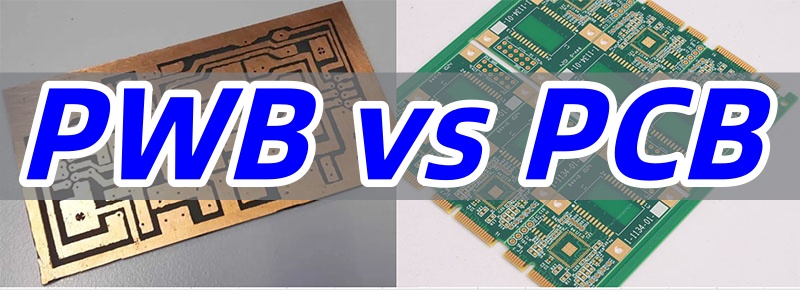
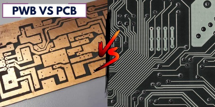
What is the Difference between PCB and PWB?
The difference between PWB (Printed Wiring Board) and PCB (Printed Circuit Board) is subtle. In modern parlance, PCB has become the universal, catch-all term. For most practical purposes, especially in globalized electronics supply chains, they are considered functionally the same. However, a closer examination of the terms highlights an evolution in the technology’s role.
| Aspect | PWB (Printed Wiring Board) | PCB (Printed Circuit Board) |
|---|---|---|
| Main idea | Wiring base | Complete circuit board |
| Focus | Simple interconnection | Circuit function + interconnection |
| Typical layers | Single / double-sided | Double-sided / multilayer |
| Typical use | Basic, low-cost electronics | Complex, high-performance electronics |
| Term usage today | Older / less used term | Modern, standard industry term |
The fundamental distinction lies in the implied scope:
- PWB focuses on the wiring—the physical infrastructure for connections.
- PCB encompasses the complete circuit—the wiring plus the integrated components and their collective function.
To sum up, a PWB is typically associated with simpler structures, while a PCB implies a more complex, multi-layered board designed for higher performance. However, it is crucial to remember that in today’s industry, the term PCB is universally accepted to describe boards of all complexity levels, from the simplest to the most advanced. The historical distinction between a printed wire board and a printed circuit board has largely faded in everyday use, with PCB emerging as the dominant term worldwide.
What are the Three Types of PCBs?
PCBs are commonly classified by their layer count, mirroring the types of PWBs:
- Single-Layer PCBs: The simplest type, with components on one side and circuitry on the opposite side.
- Double-Layer PCBs: Circuits on both top and bottom layers, connected by vias.
- Multi-Layer PCBs: Incorporate multiple layers of circuitry (4, 6, 8, up to 50+ layers), allowing for extremely complex and dense designs. This is what PCB means in electronics for advanced applications.
What is the Difference between PWB and PWA?
This distinction is more concrete. PWB vs PWA refers to different stages of production.
- PWB (Printed Wiring Board): The bare, unpopulated board.
- PWA (Printed Wiring Assembly): This is the PWB after all the electronic components have been soldered onto it. It is a fully functional circuit assembly.
What is the Difference between PWA and PCB?
Similarly, the difference between PWA and PCB is clear:
- PCB: Can refer to the bare board (like a PWB) or, generically, to the assembled board.
- PWA: Specifically and exclusively refers to the assembled board. PCBA (Printed Circuit Board Assembly) is a more common term that is synonymous with PWA.
Why is PWA not Popular?
The term PWA is not as popular as PCBA simply due to industry convention.
PCBA has become the globally accepted and more frequently used acronym for an assembled board. While PWA is technically correct, its usage has diminished over time in favor of PCBA.
Is PCBA the Same as PCA?
Yes, absolutely. PCBA (Printed Circuit Board Assembly) and PCA (Printed Circuit Assembly) are different terms for the exact same product: a fully assembled and functional circuit board. The distinction is purely terminological, with no difference in the physical item itself. The flowchart you provided elegantly illustrates the evolution and equivalence of these terms.
The diagram shows two parallel “lineages” of terminology that converge on the same meaning:
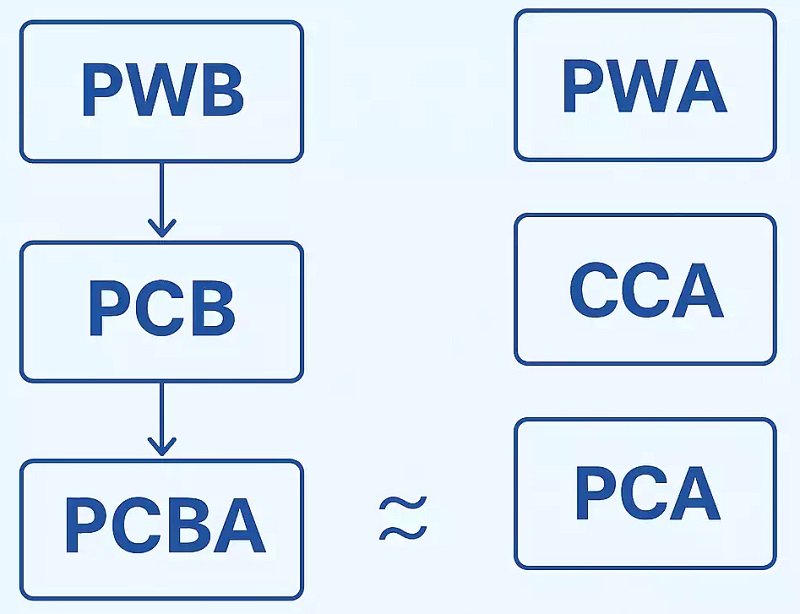
1. The Left-Hand Path: From Bare Board to Assembly (PCB Focus)
This path uses the more modern and globally dominant term “PCB” as its base.
- PWB/PCB: The process starts with the bare board, which can be called a PWB (Printed Wiring Board) or, more commonly today, a PCB (Printed Circuit Board). This is the unpopulated substrate with the copper traces.
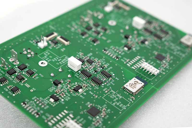
- PCBA: When all the electronic components (chips, resistors, capacitors, etc.) are soldered onto the bare PCB, it becomes a PCBA (Printed Circuit Board Assembly). This is now a complete, functional electronic sub-unit.
2. The Right-Hand Path: Alternative and Historical Terms (PWB Focus)
This path reflects terminology that is sometimes used interchangeably or is more common in specific regions or older documentation.
- PWA/CCA: If you start with the term PWB, the assembled version can be called a PWA (Printed Wiring Assembly) or a CCA (Circuit Card Assembly).
- PCA: The term PCA (Printed Circuit Assembly) is the direct equivalent of PWA and CCA.
The Crucial Link: PCBA ≈ PCA
The most important part of the chart is the “≈” (approximately equal to) symbol connecting PCBA to PCA. This symbol confirms that these two terms are functionally identical. They both describe the final product—a circuit board that has been fully assembled with components and is ready for use.
In summary, the different terms often reflect historical, regional, or company-specific preferences. For instance:
- PCB/PCBA are the most universally recognized and used terms today.
- PWB/PWA are seen as more traditional terms, still used by some companies (particularly in Japan).
- CCA is a term frequently used in the aerospace and defense industries.
- PCA is a less common but perfectly valid synonym for PCBA.
Regardless of the acronym used, they all point to the same essential item: a populated and functional circuit board. Therefore, when you see PCBA or PCA on a datasheet or in a conversation, you can be confident they refer to the same thing.
PWB vs PCB: How Each Board Fits Different Applications?
The choice between the terms PWB and PCB is largely irrelevant; the critical decision is selecting the right type of board for the application.
- For Simple, Low-Cost Applications: A single-sided PWB/PCB is often sufficient.
Examples include simple calculators, LED lights, and basic toys. - For Moderate Complexity: Double-sided boards offer a good balance of cost and functionality for products like power supplies, automotive dashboards, and industrial controllers.
- For High-Performance, Complex Applications: Multi-layer PCBs are essential.
They are used in computing hardware, telecommunications infrastructure, advanced medical devices, and any application involving high-speed digital signals or RF circuits.
Understanding the difference between printed wire board and printed circuit board terminology is less important than understanding these performance tiers.
In conclusion, PWB vs PCB are terms that, for all practical purposes, describe the essential backbone of modern electronics, with PCB being the dominant contemporary term. This article has clarified the terminology, types, and applications of these critical components to aid in your selection process.
For your PWB, PCB or PCBA projects, partnering with a reliable manufacturer is key. BEST Technology stands out as a leader in PCB manufacturing and PCBA, offering expertise from design support to full assembly (PCBA). We ensure high quality, reliability, and performance for all your electrical PCB needs. For more information or to discuss your specific requirements, please contact our expert team at sales@bestpcbs.com.
Tags: PWB vs PCB