

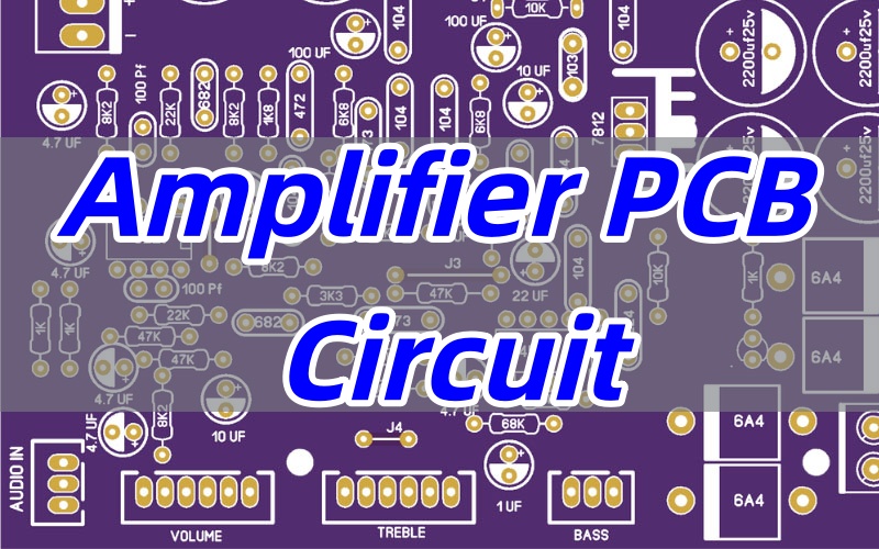
An amplifier PCB circuit is the foundational platform that houses and connects the electronic components responsible for boosting audio signals with fidelity and power. This article will explore how a well-designed amplifier circuit board is critical to achieving high-quality sound, examine common topologies, and provide key insights into layout considerations for various audio applications.
Even the best electronic components can underperform if the underlying amplifier PCB is poorly designed. Are you struggling with your audio amplifier projects due to recurring circuit board issues?
- Unwanted Noise and Hum: Poor layout can lead to ground loops and electromagnetic interference, degrading the signal-to-noise ratio.
- Thermal Management Problems: Inadequate heat sinking on the PCB causes power components to overheat, leading to failure or distorted output.
- Signal Integrity Loss: Incorrect trace routing, especially for input stages, can make the amplifier circuit board susceptible to oscillations and signal degradation.
- Power Delivery Instability: Weak power supply decoupling and thin power traces result in voltage sag during high-power demands, affecting the pcb power amplifier performance.
- Manufacturing Defects: Using inferior PCB materials or imprecise fabrication processes leads to reliability issues in the final amp circuit board.
Fortunately, these challenges can be systematically addressed through expert amplifier PCB circuit design and manufacturing. Here are the core solutions that a professional Amplifier PCB Circuit Board provider implements.
- Strategic Layout for Clean Audio: Implementing optimal grounding schemes and component placement to isolate sensitive analog sections from noise sources.
- Integrated Thermal Design: Incorporating large copper pours, thermal vias, and designated areas for heatsinks to ensure efficient cooling.
- Precision Impedance Control: Carefully designing trace widths and lengths to maintain signal integrity from input to output on the amplifier circuit pcb.
- Robust Power Plane Design: Using multilayer boards with dedicated power and ground planes to ensure stable, low-impedance power delivery.
- High-Quality Fabrication: Employing high-grade FR-4 or specialized materials with strict quality control to produce reliable and durable Amplifier PCBs.
At BEST Technology, we have specialized in manufacturing robust amplifier PCB circuits for audio applications for over 19 years. Our technical expertise ensures that your amplifier PCB circuit is built to the highest standards of reliability and electrical performance, unlocking the full potential of your PCB amplifier circuit design. Pls feel free to contact us at sales@bestpcbs.com to discuss your amplifier circuit PCB project requirements.
What Is an Amplifier PCB Circuit?
An Amplifier PCB Circuit is a specially designed printed circuit board that provides the mechanical structure and electrical connections for all components in an audio amplification system. It is much more than a simple platform; it is an integral part of the amplifier’s performance.
- The Substrate: The base material, typically FR-4, provides insulation and structural integrity. For high-power applications, materials with better thermal conductivity may be used.
- Conductive Traces: These copper pathways etched onto the board carry audio signals, power, and ground between components. Their design is critical for minimizing resistance and inductance.
- Components: The PCB hosts both through-hole and surface-mount devices (SMDs) like resistors, capacitors, transistors, and integrated circuits (ICs) such as the TDA2030 or TDA7294.
- The Layout: The spatial arrangement of components and traces is what truly defines the board’s functionality, directly influencing gain, bandwidth, and stability.
In summary, the amplifier PCB circuit is the backbone of any audio amplifier, determining its overall sound quality, efficiency, and reliability.
How an Amplifier Circuit Board Shapes Signal Gain and Output Stability?
The physical implementation of the circuit on the amplifier circuit board is paramount in realizing the theoretical performance of the schematic. A poor layout can ruin a good design.
- Gain and Signal Path:
The voltage gain of an amplifier is set by feedback components (e.g., resistors).
On the PCB, the traces connecting these components must be short and direct.
Long, looping traces can act as antennas, picking up noise and introducing parasitic capacitance, which can alter the gain, especially at high frequencies.
- Stability and Oscillation Prevention:
High-gain amplifiers can become unstable and oscillate due to unintended feedback.
A proper amplifier circuit PCB layout uses techniques like ground planes to provide a low-impedance return path and decoupling capacitors placed extremely close to the power pins of ICs to suppress high-frequency noise.
- Output Stage Integrity:
The output stage, which drives speakers, handles significant current.
The PCB traces for the output must be wide enough to carry this current without excessive voltage drop or heating.
This is especially critical in a 200w amplifier circuit diagram PCB or higher.
Therefore, a meticulously designed board is not just a convenience but a necessity for stable gain and clean, powerful output.
Key Components Found in a PCB Power Amplifier and Their Functions
Understanding the roles of key components on a PCB power amplifier is essential for both design and troubleshooting.
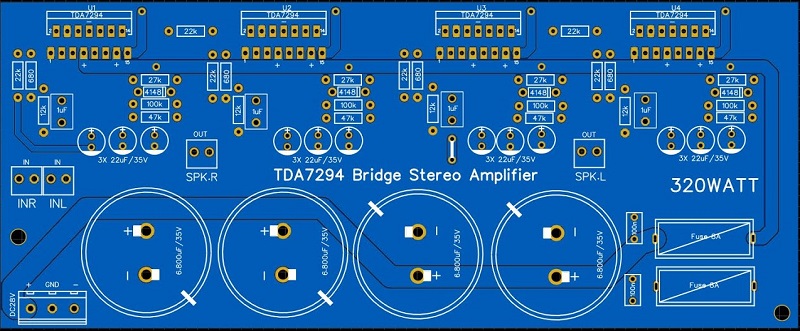
- Integrated Circuit (IC) Amplifier: Chips like the TDA2030, TDA7294, or LM3886 are the hearts of many amplifier designs, containing the core amplification circuitry in a single package.
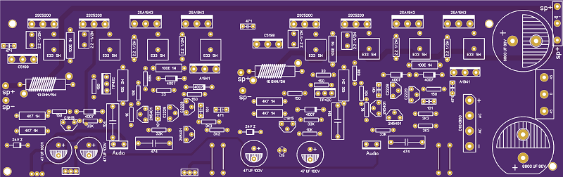
- Power Transistors: In discrete designs, bipolar transistors (e.g., 2SC5200/2SA1943 pairs) or MOSFETs are used in the output stage to deliver high current to the speaker. The c5200 a1943 amplifier circuit PCB must be designed to handle their power dissipation.
- Electrolytic Capacitors: Large-value capacitors (e.g., 1000µF+) are used in the power supply filter to smooth the DC voltage. Smaller ones (e.g., 100µF) are used for coupling audio signals between stages.
- Ceramic Capacitors: Small ceramic capacitors (0.1µF) are used for high-frequency decoupling, placed directly at the IC’s power pins to shunt noise to ground.
- Resistors: They set bias currents, determine voltage gain (in conjunction with capacitors), and provide feedback.
Each component on the power amplifier circuit PCB layout plays a specific role, and their correct selection and placement are vital for the subwoofer amplifier circuit PCB or any other audio amp to function correctly.
Understanding Common Amp Circuit Board Topologies for Audio Applications
Amp circuit board topologies refer to the structural design approaches—or architectural frameworks—used to organize how an amplifier processes, amplifies, and outputs audio signals on a PCB. Different audio applications call for different amp circuit board architectures, each with distinct advantages.
- Class AB Amplifiers: A common topology for general-purpose audio, offering a good balance between sound quality and efficiency. The tda2030 amplifier circuit diagram PCB and tda2050 amplifier circuit PCB are classic examples. They require careful biasing to minimize crossover distortion.
- Class D Amplifiers: Known for high efficiency (often >90%), making them ideal for portable and high-power systems like a 1000w amplifier circuit diagram PCB. The class d amplifier circuit PCB layout is critical, as it involves high-speed switching of MOSFETs and requires careful management of electromagnetic interference (EMI).
- Tube (Valve) Amplifiers: Prized for their warm, harmonic distortion, they require high voltages and have different PCB considerations, often involving point-to-point wiring or specialized boards.
Choosing the right topology, whether for a guitar amplifier circuit diagram with PCB layout or a home theater system, is the first step toward achieving the desired audio characteristics.
How to Read an Amplifier Circuit PCB Layout for Professional Builds?
Interpreting a layout is a key skill for troubleshooting and custom builds. When you look at a power amplifier circuit diagram with PCB layout pdf, follow these steps:
- Correlate Schematic and Layout: Identify key components (ICs, transistors) on the schematic and find their footprints on the PCB layout.
- Trace the Signal Path: Follow the input signal from the connector through each amplification stage to the output. This path should be as direct as possible.
- Identify Power and Ground Planes: Look for large areas of copper that are not etched away. These are typically ground or power planes, essential for stability.
- Check Component Orientation: Ensure polarized components like capacitors and diodes are correctly oriented according to the silkscreen layer.
Understanding a tda7294 amplifier circuit PCB layout, for instance, allows you to verify that decoupling capacitors are properly placed and the output traces are sufficiently wide.
Class D Amplifier Circuit PCB Layout Considerations for High-Efficiency Designs
The class D amplifier circuit PCB layout is arguably the most demanding. Key considerations include:
- Minimizing Parasitic Inductance: The switching loop (including the MOSFETs, output filter, and decoupling capacitors) must be as small as physically possible to reduce ringing and EMI.
- Grounding Strategy: A solid ground plane is essential. Separating analog (input) and power (output) grounds, tying them together at a single point, is a common practice.
- Component Selection: Use components rated for high frequencies, especially the output filter inductor and capacitors.
A successful layout, as seen in a quality 3kw power amplifier driver circuit PCB layout, is the difference between a clean, efficient amplifier and a noisy, unreliable one.
Subwoofer Amplifier Circuit PCB Requirements for Deep Bass Performance
A subwoofer amplifier circuit PCB must be engineered to deliver high power at low frequencies with minimal distortion.
- High Current Capacity: The PCB traces for the power supply and output stage must be very wide to handle the large currents needed for deep bass.
- Sturdy Power Supply: The design must feature robust power supply filtering to prevent “rail sag” during loud bass notes, which can cause compression and distortion.
- Stable Low-Frequency Operation: The feedback network and component values are chosen to ensure stability and optimal performance specifically in the sub-bass range (20-80 Hz). This is a key focus in a 12v subwoofer amplifier circuit PCB.
Why choose EBest Circuit (Best Technology) for Amplifier PCB Circuit Board?
When your goal is to unlock superior audio quality, the choice of amplifier circuit PCB manufacturer is critical. BEST Technology stands out for several reasons.
- Professional Expertise: We possess deep expertise in the specific demands of audio electronics, from a simple ta2030 amplifier circuit PCB to a complex mosfet power amplifier circuit diagram with PCB layout.
- High-Quality Materials & Advanced Processes: We use high-quality materials and advanced manufacturing processes to ensure excellent electrical characteristics and durability.
- Engineering Optimization Support: Our engineering support can help you optimize your amplifier circuit diagram with PCB layout for the best possible performance.
- Strict Reliability & Quality Testing: We rigorously test our Amplifier PCBs to ensure they meet your specifications and reliability expectations.
In summary, an amplifier PCB circuit is the critical link between a theoretical schematic and a high-performance audio product, directly influencing sound quality, power output, and reliability. This article has detailed the importance of the amplifier circuit board, its key components, and the layout nuances for various topologies. By prioritizing a robust amp circuit board design, you can effectively eliminate common audio issues and achieve exceptional sonic performance. At BEST Technology, we are committed to providing the high-quality, reliable amplifier PCB circuit boards that your designs deserve. For a quote or technical consultation, please contact us at sales@bestpcbs.com.
Tags: Amplifier Circuit Board, Amplifier PCB Circuit, PCB Power Amplifier