

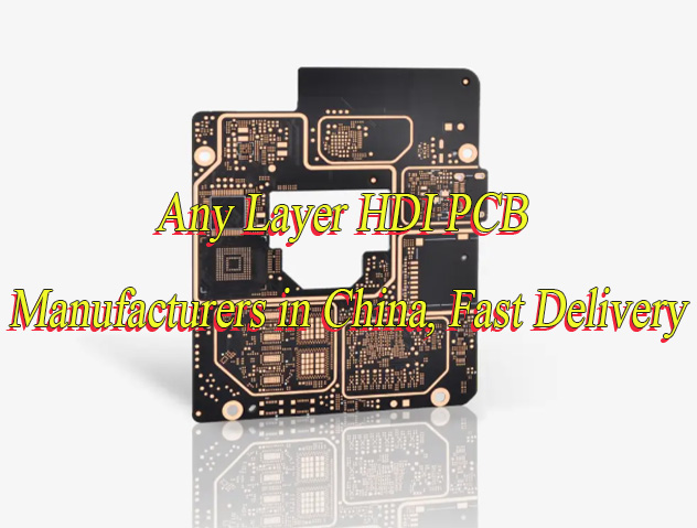
Why choose any layer HDI PCB? Let’s discover benefits, applications, design technical parameter and guide, production process, cost and supplier recommendations for any layer HDI PCB.
Are you worried about these problems?
- Is signal integrity compromised by interlayer alignment errors, delaying product launch?
- How to overcome thermal challenges from high-density routing affecting long-term stability?
- Can complex any-layer blind/buried via processes balance cost and yield for innovation?
As an any layer HDI PCB manufacturer, EBest Circuit (Best Technology) can provide you services and solutions:
- Precision Alignment, Yield Guarantee: Adopt “laser positioning + dynamic compensation” for 0.1mm interlayer accuracy, 95%+ yield stability, 30% shorter development cycles.
- Thermal Matrix, Steady Performance: Innovative “microvia heat dissipation + embedded copper foil” structure supports 200W/m² sustained cooling, ≤2% signal attenuation in high temperatures.
- Flexible Production, Cost Balance: Full-chain flexible line enables 7-day rapid prototyping and 28-day mass production transition, 15% lower small-batch costs, eliminating barriers from design to scale.
Welcome to contact us if you have any inquiry for any layer HDI PCB: sales@bestpcbs.com.
What Is Any Layer HDI PCB?
Any Layer HDI PCB (Any Layer High Density Interconnect Printed Circuit Board) is a revolutionary PCB manufacturing technology. It utilizes laser drilling to create micron-scale microvias on all conductive layers of the circuit board, including the innermost layers, combined with an electroplating via-filling process.
This enables direct interconnection between any two adjacent circuit layers, eliminating the dependency on mechanically drilled through-holes for interlayer connections. Consequently, it breaks free from the limitations of traditional through-holes and conventional buried/blind via stacking structures in standard HDI designs, achieving the most advanced routing density and ultra-compact design capabilities currently attainable.
Why Choose Any Layer HDI PCB Board?
Advantages of Any Layer HDI PCB Board:
- Extreme miniaturization for market leadership: Saving 30%-50% of device space to enable slimmer, lighter products such as foldable smartphones and AR glasses, directly boosting terminal product competitiveness and premium pricing power.
- Flagship performance for enhanced user experience: Supporting ultra-high-speed signals like 5G/6G millimeter wave and PCIe 5.0 with zero-latency data transmission; reducing power consumption by 15% to extend device battery life and elevate user satisfaction.
- High-density integration for reduced system complexity: Integrating CPU/GPU/memory on a single board to minimize connectors and cables, cutting system failure rates by 20% and optimizing production costs by 10% through material and assembly savings.
- Enhanced reliability for lower after-sales costs: Copper-filled via technology triples thermal cycle resistance, achieves over 99% pass rates in vibration tests, reduces warranty repair rates by 40%, and significantly cuts after-sales expenses.
- High design freedom for faster time-to-market: Any-layer interconnection breaks routing constraints to shorten R&D cycles by 30%, enabling rapid market response and capturing prime sales windows.
- Advanced packaging support for technical barriers: Compatible with 0.3mm pitch BGA and SiP packaging for chip-level integration, creating a technological moat to differentiate from competitors.
- Future-proof scalability for long-term investment: Reserving 10+ layer high-density routing space to support future upgrades like AI modules, avoiding sunk costs from redesigns within 1-2 years.
When to Use Any Layer HDI PCB?
Applications of Any Layer HDI PCB:
- Consumer Electronics: High-end smartphones and tablets (e.g., iPhone, Huawei Mate series), wearable devices (smartwatches, wireless earphones), and ultra-thin laptops.
- Communication and 5G Infrastructure: 5G base stations and RF modules, satellite communication equipment (low-orbit satellites).
- Automotive Electronics and Intelligent Driving: Advanced Driver Assistance Systems (ADAS) including radar and camera modules, in-vehicle infotainment and electronic control systems (autonomous driving assistance, battery management), electric vehicle power drive control units.
- Medical and Life Sciences: High-precision medical equipment such as MRI machines, CT scanners, portable ultrasound devices, and implantable devices like pacemakers and nerve stimulators.
- Aerospace and Defense: Satellite and spacecraft communication modules, attitude control systems, military electronic equipment (radar, tactical communication).
- Industrial Automation and High-Performance Computing: Industrial control devices (PLCs, robot controllers), data centers and servers (high-performance computing units, high-speed storage modules).
- Other High-Demand Scenarios: Scientific research instruments (particle accelerators, precision measurement equipment), high-end consumer electronics (gaming consoles, professional cameras).
Any Layer HDI PCB Design Technical Parameter
| Design Parameter | Typical Value/Range |
| Layer Range | 4-68 layers (mainstream 8-24 layers) |
| Minimum Line Width/Spacing | 3-40μm (3-4mil) |
| Laser Drilling Diameter | 0.075-0.15mm |
| Microvia Aspect Ratio | ≤1.25:1 |
| Material Type | FR-4/Rogers/MEGTRON/ABF |
| Copper Thickness Range | Outer layer 1-30oz, Inner layer 0.5-30oz |
| Surface Finish | ENIG/OSP/Immersion Silver |
| Signal Integrity | ≤10% impedance control |
| Thermal Management | Thermal shock ≥1000 cycles (-55°C to +125°C) |
| Reliability Testing | Insulation resistance ≥10MΩ |
| Routing Density | >20 pads/cm² |
| Tolerance Control | ±7% line width/hole diameter |
| Lamination Process | Vacuum lamination |
How to Design Any Layer HDI PCBs?
1. Layer Stackup and Impedance Control
- Core Principle Upgrade: Employ dynamic stackup optimization algorithms to automatically adjust layer counts based on signal density distribution (e.g., 8-layer boards use L1-L2 signal/ground hybrid layers + L3-L6 buried capacitance layers + L7-L8 signal layers). Thin dielectric layers (30-50μm) require precise impedance calibration using 3D field solvers, targeting 50±5%Ω for single-ended signals and 90-110Ω for differential pairs, supporting over 100GHz high-frequency signal transmission.
- Impedance Formula Expansion: Introduce nonlinear material models (e.g., Debye model) to correct high-frequency effects. Microstrip impedance Z0=εr87ln(0.8w+t5.98h) requires skin-effect correction terms, while striplines must account for coupling capacitance between adjacent copper layers. Reserve ±5% manufacturing tolerance, with differential impedance control for critical signal lines.
- Material Selection Deepening: For high-frequency scenarios, LCP (liquid crystal polymer) substrates (Dk=2.9, Df=0.002) are recommended. Medical devices require ISO 10993 biocompatibility certification, while automotive electronics select materials with matched CTE (CTE difference <5ppm/℃) to ensure reliability under -55℃~150℃ thermal cycling.
2. Application of Blind and Buried Via Technologies
- Blind Via Design Advancement: Utilize UV laser + CO₂ laser hybrid drilling to achieve diameters down to 50μm with depth control accuracy of ±2μm. Blind via bottoms require plasma cleaning + chemical copper deposition to ensure void-free walls, reducing wiring space by 40% and enabling 3D stacked packaging.
- Buried Via Process Breakthrough: Implement step-laminate + electroplating fill + chemical polishing to achieve void-free filling of 0.05mm ultra-fine vias. Buried via matrices must avoid high-frequency signal paths to minimize crosstalk. X-ray inspection verifies fill quality with porosity <1%.
- Reliability Verification Enhancement: Pass -60℃~150℃ rapid thermal cycling test (1000 cycles) with copper fracture rate <0.005%. AI-based visual inspection systems monitor via dimensions in real-time, adjusting drilling parameters dynamically.
3. Signal Integrity Optimization
- Routing Strategy Upgrade: High-speed signals adopt serpentine routing + differential pair coupling. DDR5 requires ±2mil length tolerance, limiting via count to ≤2 per signal path. Low-loss materials (Df<0.003) reduce dielectric loss, with reference ground via arrays (spacing 50mil) added to critical signal lines.
- Simulation Verification Deepening: Perform full-chain SI/PI simulation using Ansys HFSS/Sigrity. TDR impedance continuity must meet ±3% tolerance. Optimize crosstalk suppression (<3%) and return loss (<7%) for signals >100Gbps, with 3D EM field simulation verifying EMI/EMC compliance.
- Grounding Design Innovation: Implement gridded ground planes + embedded capacitors to reduce eddy current losses. Power-ground spacing ≤2mil, with integrated heat-shield copper arrays beneath critical ICs.
4. Thermal Management Solutions
- Thermal Design Breakthrough: Use metal-matrix composites (e.g., AlSiC) or graphene-enhanced FR-4 with thermal conductivity >5.0W/mK. 3D thermal via arrays (diameter 0.2mm, pitch 3mm) beneath high-power components (e.g., GPUs) combined with micro heat pipes/vapor chambers reduce core temperatures by 8℃.
- Layout Optimization Strategy: Adopt “hot-cold” zoning for heat-generating components, avoiding local thermal density >3W/cm². Maintain >800mil spacing between power modules and sensitive circuits, using thermal isolation trenches + thermal adhesive to reduce coupling. Thermal simulation software optimizes heat dissipation paths, ensuring hotspot temperatures <85℃.
5. Design for Manufacturing (DFM)
- Process Specification Refinement: Minimum trace width/spacing ≤75μm, via diameter >0.08mm. Confirm laser drilling precision (<2μm), lamination alignment (<3μm), and plating uniformity (thickness deviation <8%) with manufacturers. V-cut + stamp hole depaneling reduces mechanical stress damage.
- Panelization Optimization Strategy: AI-driven panelization algorithms improve substrate utilization (>95%) using sub-panel + rotation layouts to minimize waste. Surface finishes recommend ENIG or OSP over HASL to avoid bridging risks. Critical nets include virtual breakpoints for flying probe testing.
- Testability Enhancement: Reserve test point matrices (spacing ≥80mil) with JTAG boundary scan for in-circuit testing. Add impedance monitoring points to critical signal lines for real-time manufacturing feedback.
6. Material and Reliability Verification
- Material Selection Deepening: High-frequency applications use PTFE/ceramic hybrid substrates (Dk=2.5-3.0). Automotive electronics select CTE-matched materials (CTE difference <3ppm/℃). Pass moisture absorption (<0.3%), chemical resistance, and thermal stress tests (260℃ reflow 10x without delamination).
- Reliability Testing Enhancement: Include thermal shock (1000 cycles), vibration (IEC 60068-2-64), electrochemical migration, and bending tests (5mm radius no fracture). Medical devices require ISO 10993-1 biocompatibility and sterilization compatibility certifications.
7. Simulation and Verification Process
- Design Verification Upgrade: Perform multi-physics simulations (Altium Designer/Cadence) to validate signal integrity, power integrity, thermal distribution, and mechanical stress. Thermal imaging + IR sensors monitor hotspots in real-time, optimizing heat paths. 3D X-ray inspects interlayer alignment and via fill quality.
- EMC Compliance Strategy: Triple shielding with cavities + filter capacitors + common-mode chokes ensures CISPR 32/FCC Part 15 Class B compliance. Critical interfaces (e.g., USB4/PCIe 5.0) add differential/common-mode filtering circuits to suppress >100MHz radiation noise.
- Documentation Output Specification: Generate IPC-A-600/IPC-6012-compliant Gerber files, BOMs, and process specifications. Include stackup tables, impedance control reports, thermal simulation results, and reliability test reports to ensure design traceability and manufacturing consistency.
How to Make Any Layer HDI PCBs?
1. Design Planning and Verification
- Impedance Control and Signal Integrity: Utilize high-frequency simulation tools (such as ADS, HFSS) for signal integrity analysis to ensure transmission line impedance matching (e.g., 50Ω single-ended traces, 100Ω differential pairs). Verify impedance consistency via TDR testing with deviation ≤±10%.
- DFM/DFA Advanced Verification: Leverage DFM software to check design file compatibility, avoiding blind/buried via misjudgment. Execute 29 bare-board inspection rules (e.g., minimum trace width/spacing 50μm verification, pad size tolerance ±0.05mm) and 800 PCBA assembly rule validations.
- 3D Modeling and Thermal Design: Build 3D models via Altium Designer’s layer stack manager to analyze CTE mismatch (layer-to-layer CTE difference ≤10ppm/℃). Simulate thermal cycling stress distribution to optimize heat dissipation paths.
2. Material Selection and Pretreatment
- Substrate Characteristic Matching: For high-frequency applications, select low-Dk/Df materials (e.g., PTFE with Dk=2.5–3.0, Df<0.005). For high-temperature scenarios, use high-Tg FR-4 (Tg≥170℃). Flexible HDI boards require polyimide substrates with flexural strength 300–500MPa.
- Copper Foil and Prepreg Optimization: Inner layers adopt rolled copper foil (surface roughness Ra<0.3μm) to minimize signal loss. Outer layers use 1–3oz copper based on current density. Prepreg must match substrate CTE and control resin flow (e.g., low-flow PP for fine-line solder mask resistance).
- Surface Treatment Processes: Control ENIG thickness at Ni 3–5μm/Au 0.05–0.1μm. OSP thickness ranges 0.2–0.5μm. ENEPIG requires uniform Pd layers to enhance solder joint reliability.
3. Inner Layer Fabrication and Pattern Transfer
- Pattern Transfer Accuracy Control: Achieve ±5μm line precision via LDI laser direct imaging. Maintain dry film exposure energy precision ±0.5mJ/cm² and develop line width deviation ≤±3μm.
- Etching and AOI Inspection: Acidic etching solutions (e.g., CuCl₂+HCl) operate at 45±2℃ with time precision ±5 seconds. AOI detects line width/spacing defects at <0.1 defects/cm² and performs automatic short/open repair.
- Oxidation Treatment Process: Black hole/brown oxidation controls layer thickness 0.1–0.3μm, ensuring interlayer peel strength >1.5N/mm. X-ray inspects hole position offset ≤25μm.
4. Drilling and Hole Metallization
- Laser Drilling Parameter Optimization: UV laser (3–15W) drills <75μm microvias with 10–30μm spot diameter. CO₂ laser (10–50W) drills ≥100μm holes at 20–80kHz pulse frequency with 0.1–0.3MPa nitrogen assistance.
- Mechanical Drilling and Deburring: Monitor drill bit wear ≤0.02mm for large holes (>0.2mm). Post-drilling plasma cleaning removes smear. Hole wall roughness Ra≤2μm.
- Copper Plating and Electroplating Processes: Chemical copper deposition thickness 0.5–1.0μm. Electroplated copper thickens to 20–30μm. CT scanning ensures >99% void-free holes with conductivity resistance change <5%.
5. Lamination and Layer Alignment
- Vacuum Lamination Process: Control temperature profiles in stages (pre-press 100–130℃/10min, main press 180–200℃/2h). Pressure ramps from 50psi to 400psi to ensure >95% resin fill rate.
- Layer Alignment Accuracy: X-ray drilling targets achieve ±25μm alignment accuracy. Secondary element measurement verifies layer thickness deviation ≤±3%.
- Thermal Stress and Warpage Control: Symmetrical layer structures reduce internal stress. Post-curing (150℃/2h) enhances dimensional stability with warpage ≤0.5%.
6. Outer Layer Fabrication and Surface Treatment
- Outer Layer Pattern Transfer and Etching: Replicate inner layer processes with ±5μm line precision. AOI detects defects at <0.1 defects/cm².
- Solder Mask and Legend Printing: Solder mask thickness 20–30μm with exposure energy precision ±0.5mJ/cm². UV-cured inks ensure >50 friction test cycles for legend durability.
- Surface Treatment Validation: Salt spray testing (48h no corrosion) and thermal shock testing (-55℃/125℃ for 1000 cycles) verify surface treatment reliability.
7. Testing and Quality Control
- Electrical Performance Testing: Flying probe testers detect opens/shorts with impedance deviation ≤±10%. ICT validates component solder reliability with joint failure rate <0.1%.
- Reliability Test Standards: Temperature cycling (-40℃ to 125℃ for 1000 cycles) ensures microvia resistance change <10%. Humidity aging (85℃/85% RH/1000h) maintains insulation resistance >10⁹Ω.
- Vibration and Shock Testing: Random vibration (5–2000Hz/10G for 100h) maintains 100% microvia conductivity. Mechanical shock (50G/11ms) for 3 cycles results in no solder joint failure.
8. Packaging and Shipment
- Eco-Friendly and Anti-Static Packaging: Utilize anti-static foil bags (surface resistance <10¹¹Ω) with vacuum sealing. Include humidity indicator cards (threshold <5%RH) and maintain transport temperature 5–35℃.
- Traceability and Quality Documentation: Each batch includes QC reports (AOI/X-ray/electrical test data). Barcode traceability tracks full production parameters per IPC-6012/AEC-Q100 standards.
- Final Pre-Shipment Inspection: Sample 5 units for 100 temperature cycles + 100h humidity aging with 100% pass rate before release.
How Much Does Any Layer HDI PCBs Cost?
| Category | Cost Range (USD) |
| Basic any-layer HDI (4-6 layers) | $50–$200 per sq ft |
| Mid-range HDI (6-8 layers) | $200–$500 per sq ft |
| High-complexity HDI (8+ layers, ultra-fine pitch) | $500–$1,500+ per sq ft |
| Prototype/small batch (per board) | $100–$1,000+ per board (complexity-dependent) |
Why Choose EBest Circuit (Best Technology) as Any Layer HDI PCB Manufacturer?
Reasons why choose us as any layer HDI PCB manufacturer in China:
- 19 Years of Technical Accumulation Trusted by Industry Leaders: With 19 years of expertise in HDI PCB manufacturing, we’ve served over 200 Fortune 500 companies across consumer electronics, automotive, and medical sectors. Our proven technical maturity and reliable delivery ensure your projects are in safe hands.
- Global Certifications Ensuring Compliance and Trust: Certified with ISO13485, RoHS, AS9100D, and IATF16949, our products meet stringent global standards for medical, aerospace, automotive, and environmental compliance. Expand into premium markets with confidence.
- Free DFM Optimization Cutting Development Costs by 30%: Our complimentary Design for Manufacturability (DFM) service proactively identifies design flaws and optimizes layouts, reducing prototyping iterations and costs. This accelerates time-to-market while lowering R&D expenses by up to 30%.
- One-Stop Service Saving Time and Resources: From PCB design and engineering evaluation to material sourcing, manufacturing, and logistics, our end-to-end service eliminates coordination hassles with multiple vendors. Focus on core business while we handle the rest.
- Competitive Pricing with Uncompromised Quality: Leveraging scaled production and vertically integrated supply chains, we offer industry-leading pricing, 15% to 25% lower than comparable solutions without sacrificing quality, maximizing your product margins and market competitiveness.
- Multi-Layer Quality Control Exceeding Industry Standards: Our triple-layer quality system includes raw material testing, in-process monitoring, and final inspection using AOI and X-ray technologies. Defect rates stay below 50ppm, surpassing IPC Class 2 benchmarks for superior reliability.
- 48-Hour Rapid Prototyping for Faster Market Entry: Our industry-leading turnaround time delivers standard HDI prototypes within 48 hours, supporting urgent prototyping and small-batch trials. Accelerate design validation and seize market opportunities ahead of competitors.
- Precise and Flexible Delivery Times: Smart production scheduling and agile capacity management enable 5-7 day standard lead times, with urgent orders deliverable in as little as 3 days. Seamlessly transition from prototyping to volume production as your needs evolve.
Welcome to contact us if you have any request for any layer HDI PCB: sales@bestpcbs.com.