

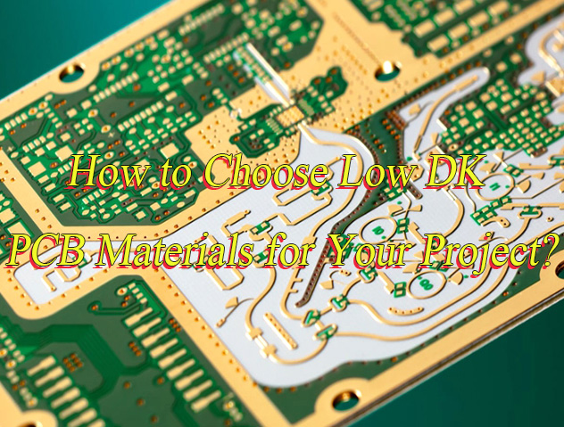
How to choose low DK PCB materials? Let’s discover its definition, material list, selection guide, material properties, common material supplier together.
Are you troubled with these questions?
- How to overcome signal attenuation in high-frequency scenarios to break through rate bottlenecks?
- How to stabilize millimeter-wave module performance amid heat dissipation challenges?
- How to improve yield loss caused by impedance mismatch in multi-layer boards?
As a PCB material supplier, EBest Circuit (Best Technology) can provide you service and solution:
- Precision Material Tuning – Dual Dk/Df control technology for high frequencies, achieving ≤0.002 loss at 10GHz, 20% speed boost, and 30% lower loss.
- Smart Process Adaptation – Full-chain process parameter database with AI matching system, cutting production line upgrade time by 40% and first-pass yield by 50%.
- Digital Twin Validation – AI-powered signal integrity simulation platform predicting 95% of impedance/crosstalk risks early, boosting yield by 50% with zero additional tuning costs.
Welcome to contact us if you have any request for PCB material: sales@bestpcbs.com.
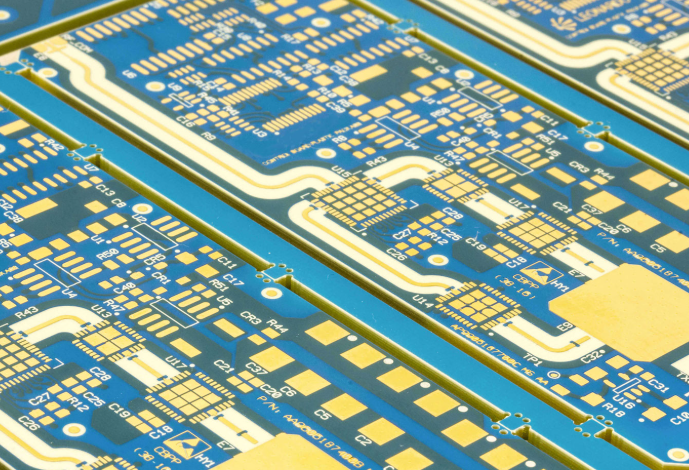
What Are Low DK PCB Materials?
Low DK PCB materials are specifically designed for high-speed and high-frequency circuits, featuring a dielectric constant (DK) typically ranging from 2 to 4, which is lower than conventional PCB materials like FR-4. This low DK characteristic significantly enhances signal transmission speed, reduces delay and distortion, and optimizes impedance control, making them widely used in 5G communications, high-speed servers, millimeter-wave radars, and other applications demanding stringent signal integrity.
How to Choose Low DK PCB Materials?
Below is a selection guide for low DK PCB material:
1. Define Application Scenarios and Core Requirements
- High-frequency/high-speed scenarios (e.g.,RF modules): Prioritize materials with DK ≤ 3.0 and Df ≤ 0.005 (e.g., PTFE substrates with DK=2.1–2.5, ceramic-resin composites with DK=2.8). For instance, 28GHz millimeter-wave antenna PCBs require PTFE substrates, which reduce signal loss by 70% compared to FR-4 and maintain impedance stability within ±0.8%.
- High-power scenarios (e.g., power amplifiers): Focus on thermal conductivity and voltage resistance. Ceramic substrates (e.g., Al₂O₃, AlN) offer thermal conductivity of 170–230W/m·K, far exceeding FR-4’s 0.3–0.4W/m·K, making them ideal for high-power dissipation.
- Harsh environment scenarios (e.g., automotive electronics): Select materials with high temperature resistance, moisture resistance, and chemical corrosion resistance (e.g., polyimide films with Tg ≥ 250°C and moisture absorption ≤ 0.6%).
2. Screen Low DK Material Types and Characteristics
- PTFE (Polytetrafluoroethylene): DK=2.1–2.5, Df=0.0002–0.0012. Ideal for high-frequency RF circuits but requires specialized processing and has higher costs.
- Ceramic Substrates: DK=2.8–3.8, excellent thermal conductivity. Suitable for high-power and high-heat-dissipation applications but prone to brittleness, requiring mechanical strength considerations.
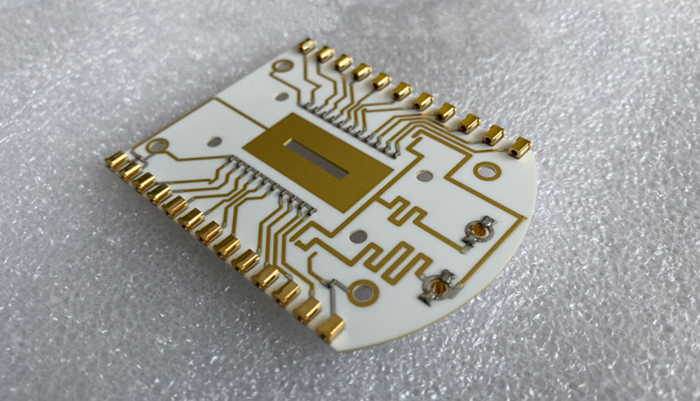
- Polyimide (PI): DK=3.1–3.7, Df=0.001–0.005. Combines flexibility and high-temperature resistance, ideal for flexible PCBs (e.g., wearables, automotive electronics).
- Low DK Glass Fiber Cloth: E.g., NE glass fiber cloth (DK=3.0–3.5). Suitable for multilayere and HDI boards with moderate cost.
3. Evaluate Parameters and Technical Specifications
- DK & Df: For high-frequency scenarios, strict control of DK ≤ 3.0 and Df ≤ 0.005 is required; for mid-to-low-frequency scenarios, relaxed to DK ≤ 4.8 and Df ≤ 0.02.
- Thermal Performance: Tg ≥ 150°C (FR-4) or ≥ 250°C (polyimide). CTE (coefficient of thermal expansion) must match copper foil (≤ 20ppm/°C) to avoid delamination under thermal stress.
- Mechanical Performance: Tensile strength ≥ 80MPa, bending radius ≤ 5mm (for flexible boards).
- Environmental Reliability: Must pass RoHS compliance, moisture absorption ≤ 1%, and chemical corrosion resistance (e.g., acid/alkali environments).
4. Environmental and Sustainability Assessment
- Material Recycling and Reuse: Prioritize recyclable or biodegradable materials (e.g., polylactic acid-based composites) to minimize e-waste. For example, certain low DK glass fiber cloths achieve >90% material regeneration via chemical recycling processes.
- Regulatory Compliance: Ensure materials meet RoHS, REACH, and other environmental regulations. The EU mandates cadmium content ≤ 0.01% in PCB materials post-2025.
- Carbon Footprint and Lifecycle Analysis: Select suppliers with transparent supply chains and low carbon footprints. Localized production reduces transportation emissions. Water-soluble solder masks can cut VOC emissions by >50%.
- Circular Economy Models: Implement closed-loop systems (e.g., “design-produce-recycle-regenerate”) by partnering with professional recycling agencies to reuse copper, resin, and other materials.
5. Cost and Supply Chain Evaluation
- Premium Materials (e.g., Rogers 4003C, PTFE): High costs but essential for extreme performance scenarios (e.g., 5G base stations). Balance performance and cost.
- Mid-tier Materials (e.g., modified FR-4, low DK glass fiber cloth): Moderate costs for consumer electronics. Optimize costs via supplier collaboration (e.g., Honghe Technology’s low DK glass fiber cloth price surge >50%).
- Supplier Selection: Prioritize certified suppliers (e.g., Japan’s Nittobo, Taiwan’s Nan Ya Plastics) for material stability and supply reliability.
6. Manufacturing Process Compatibility Verification
- HDI Boards: Use low CTE materials (≤ 20ppm/°C) to avoid layer misalignment (±0.01mm causing DK deviation of 0.02) and ensure impedance stability.
- Flexible and Rigid-Flex Boards: Select highly flexible materials (e.g., 25μm polyimide film with bending radius ≤ 1mm) and validate bonding strength with rigid materials.
- Processing Performance: Test drilling, etching, and plating capabilities to achieve >95% yield rates and avoid material-related defects.
7. Testing & Validation & Iterative Optimization
- Lab Testing: Validate signal loss and impedance matching via vector network analyzer S-parameter measurements (e.g., S21, S11). Verify thermal and reliability performance through thermal cycling tests.
- Field Testing: Conduct long-term tests in target environments (e.g., high temperature/humidity, vibration/impact) to confirm material stability.
- Iterative Optimization: Adjust material types or parameters (e.g., supplier changes, laminate process optimization) based on test results to finalize the optimal solution.
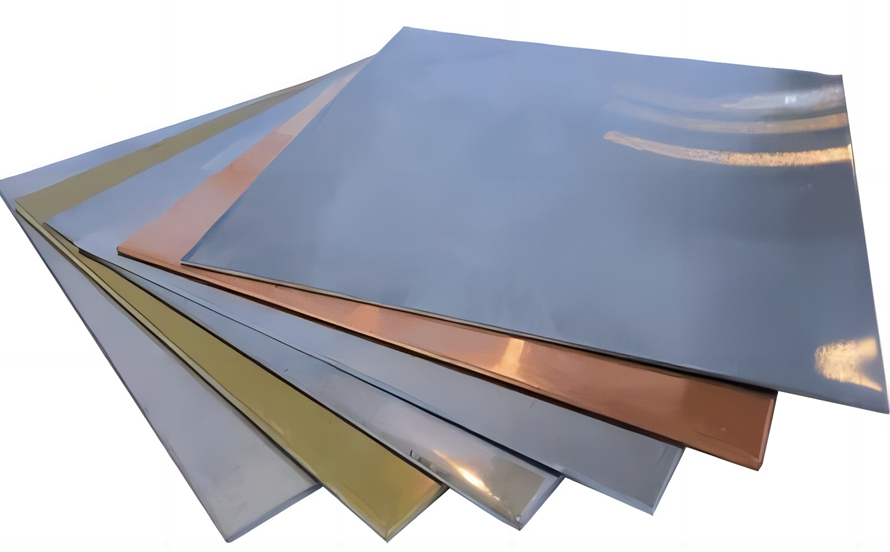
Common Low DK PCB Materials List
| Material Type | Representative Model | Dk Value Range | Loss Factor (Df) | Characteristics & Applications |
| PTFE-based Materials | Rogers RO3003™ | 3.00 ±0.04 | 0.0013 @10GHz | Ultra-low loss, millimeter-wave radar/satellite communications (77GHz) |
| PTFE-based Materials | Taconic RF-35™ | 3.50 ±0.05 | 0.0018 @10GHz | High frequency stability, 5G base station antennas |
| Modified Epoxy Resin | Panasonic Megtron 6™ | 3.70 @1GHz | 0.002 @1GHz | Cost-effective choice, 100Gbps server/switch motherboards |
| Modified Epoxy Resin | Isola FR408HR™ | 3.65 @1GHz | 0.010 @1GHz | Compatible with FR-4 process, medium-high speed network devices |
| Ceramic-filled Materials | Rogers RO4350B™ | 3.48 ±0.05 | 0.0037 @10GHz | Thermal conductivity 0.6W/mK, high-power RF amplifiers |
| Liquid Crystal Polymer (LCP) | Rogers ULTRALAM 3850™ | 2.90 @10GHz | 0.0025 @10GHz | Flexible substrate, 5G smartphone AiP antennas/millimeter-wave modules (<0.2% moisture absorption) |
| Polyimide (PI) | DuPont Kapton® HN | 3.40 @1kHz | 0.002 @1kHz | High temperature resistance (>260℃), aerospace flexible circuits |
| PPO/PPE-based Materials | Nelco N7000-2HT™ | 3.20 @1GHz | 0.0015 @1GHz | Low moisture absorption (0.2%), high-speed backplanes |
Low Dielectric Constant PCB Material Properties
- Dielectric Constant (Dk): Typical range: 2.0-3.5 (e.g., PTFE substrate Dk ≈ 2.2; PI substrate Dk ≈ 3.0-3.5), lower than conventional FR-4 (Dk ≈ 4.2-4.8). Reduces signal transmission delay and capacitive coupling crosstalk.
- Dissipation Factor (Df): For high-frequency materials like Rogers RO4350B, Df ≤ 0.003; PTFE substrate Df as low as 0.0002. Minimizes signal energy loss and attenuation in high-frequency scenarios.
- Frequency Band Stability: Dielectric constant remains stable across frequencies (weak dispersion effect), e.g., ceramic substrates maintain consistent Dk over wide bands, ensuring parameter consistency in high-frequency circuits.
- Coefficient of Thermal Expansion (CTE): Typical value ≤ 50ppm/℃, matching silicon chip CTE. Reduces interlayer stress and solder joint failure risks caused by temperature fluctuations, suitable for extreme temperature environments.
- Thermal Resistance: Materials like PI withstand short-term peak temperatures above 250°C, compatible with reflow soldering; ceramic substrates offer superior high-temperature performance for demanding scenarios.
- Chemical Corrosion Resistance: PTFE and fluoropolymers resist acid/alkali and solvent erosion, ideal for harsh environments like industrial controls or outdoor devices, extending service life.
- Mechanical Strength & Flexibility: Rigid materials (e.g., ceramic, glass-fiber reinforced substrates) provide high bending strength and dimensional stability; flexible materials (e.g., PI, PTFE composite films) support bending needs for foldable/wearable devices.
- Low Moisture Absorption: Materials like PTFE have moisture absorption < 0.01%, preventing Dk/Df drift from humidity changes and ensuring stable signal transmission in humid environments.
Why Is Low DK So Important?
- Improving Production Efficiency: The stable dielectric properties of low DK materials optimize impedance control, streamline PCB design processes, reduce debugging and validation steps, and shorten time-to-market. This helps customers seize market opportunities faster.
- Enhancing Product Competitiveness: Utilizing low DK materials enables your end devices, such as 5G smartphones and high-speed servers to achieve faster data transmission and more stable signals. This directly elevates product performance, helping your offerings stand out in the market and attract high-end customers.
- Reducing Long-Term Operational Costs: Low DK materials minimize signal loss and equipment failure rates, lowering repair and replacement costs caused by signal distortion. Their thermal stability and low moisture absorption also reduce performance fluctuations from environmental changes, extending device lifespan and saving maintenance expenses.
- Ensuring Signal Reliability: In high-frequency scenarios like millimeter-wave radar and RF front-ends, low DK materials guarantee delay-free and distortion-free signal transmission. This prevents product failures or degraded user experiences due to signal issues, boosting customer trust.
- Adapting to Future Tech Demands: As technologies like 5G/6G, AI computing, and autonomous driving evolve, high-frequency and high-speed applications demand higher signal transmission standards. Adopting low DK materials future-proofs your devices, avoiding rapid obsolescence and protecting customer investments.
What PCB Material Has the Lowest Dielectric Constant?
Boron nitride (BN) currently has the lowest dielectric constant among PCB materials (usually less than 3.0, and some modified products can be as low as below 2.0). Its ultra-low dielectric loss characteristics make it an ideal choice for high-frequency and high-speed circuits, microwave communications, and precision sensors. The porous structure of boron nitride can also suppress electromagnetic interference, regulate radio frequency signals, and is suitable for gas sensors, pressure detectors and other scenarios.
Compared with traditional materials (such as PTFE about 2.1 and FR4 about 4.5), boron nitride performs better in low-impedance connection, signal integrity and thermal stability. It is one of the core materials for 5G base stations, aerospace electronic equipment and high-performance computing chip packaging, and meets the needs of international customers for high-precision, low-loss PCBs.
Common Low Dielectric Constant PCB Materials Supplier
Below are suppliers list for low dielectric constant PCB materials:
Rogers Corporation
- Product Features: Leader in high-frequency materials, RO4000® series (hydrocarbon/ceramic) and RO3000® series (PTFE/ceramic) renowned for ultra-low loss factor (Df ≤ 0.003) and stable dielectric constant (Dk 2.0-3.5).
- Applications: 5G base station antennas, automotive radar, high-speed digital circuits (100Gbps+ transmission).
DuPont
- Product Features: Deep technical accumulation in low-Dk materials, fluoropolymer substrates (Dk ≈ 2.2) with high temperature/chemical resistance.
- Applications: High-frequency PCBs, semiconductor packaging, industrial control devices.
Amphenol
- Product Features: High-performance PTFE-based materials (e.g., TacLam® Plus) with ultra-low loss (Df as low as 0.0002) and excellent batch consistency.
- Applications: Phased-array radars, aerospace, high-speed backplanes.
Isola
- Product Features: Tachyon® 100G optimized for ultra-high-speed transmission (Dk 3.0-3.5); FR408HR® balances performance and processability.
- Applications: Data centers, 5G base stations, mixed-signal designs.
Panasonic
- Product Features: Megtron® series (e.g., Megtron 6/7/8) known for ultra-low transmission loss, CAF resistance (anti-chemical corrosion), Dk 3.0-4.0.
- Applications: High-end servers, data center high-speed backplanes, automotive electronics.
Hitachi/Showa Denko Materials
- Product Features: Low-Dk glass fiber formulations, high-frequency/high-speed materials (e.g., IC substrate), stable Dk and high-temperature resistance.
- Applications: Automotive electronics, telecom equipment, industrial controls.
Taconic
- Product Features: RF series (e.g., RF-35, RF-60) and TLY™ ultra-low-loss materials, PTFE-based, Dk 2.2-2.5.
- Applications: Millimeter-wave antennas, satellite communications, high-power amplifiers.
Asahi Kasei
- Product Features: Composite material technology, low-Dk glass fiber modification, optimized high-frequency performance and mechanical strength.
- Applications: Advanced packaging substrates, 5G infrastructure, automotive electronics.
Nan Ya Plastics
- Product Features: Full supply chain (glass fiber-epoxy-copper clad laminate), significant cost advantage, Dk 3.0-4.0.
- Applications: Consumer electronics, automotive electronics, industrial controls.
AT&S
- Product Features: High-end HDI and IC substrates, low-Dk materials (Dk 3.0-3.5), high-precision routing.
- Applications: Semiconductor packaging, high-end servers, medical devices.
Why Choose EBest Circuit (Best Technology) as Low DK PCB Materials Supplier?
Reasons why choose us as low DK PCB materials supplier:
- Precise Control of Material Performance: As a specialized material supplier, we focus on R&D of low DK PCB substrates with dielectric constant strictly controlled within 2.8-3.2 (tolerance ≤0.05) and loss factor ≤0.002. This ensures 40% improvement in signal integrity for high-frequency circuit designs, directly reducing post-debugging costs for clients.
- Supply Chain Resilience Assurance: Through exclusive partnerships with global top-tier substrate manufacturers and three intelligent warehousing centers in China, we achieve dynamic inventory management. This supports 24-hour emergency delivery with an annual supply capacity exceeding 5 million sheets, eliminating production line downtime risks caused by material shortages.
- Complimentary Technical Consulting Services: Our team of 15 senior material engineers provides end-to-end technical support covering material selection, impedance matching, and stack-up design optimization. This has helped clients reduce design iterations by 30% and shorten time-to-market by 20% on average.
- Transparent Cost Optimization Solutions: Through economies of scale and formulation optimization, we deliver 10-15% material cost savings with detailed cost-benefit analysis reports, ensuring every investment translates into performance enhancement or cost efficiency.
- Strict Batch Consistency Control: ISO 9001-certified full-process quality control includes six inspection procedures (e.g., real-time dielectric constant monitoring, thermal stress testing), ensuring batch-to-batch performance variation ≤0.05. This minimizes yield fluctuations caused by material inconsistencies.
- Customized Material Development Capability: We offer tailored material development for specialized requirements such as ultra-low loss or high thermal stability. Three proprietary low DK material variants have been successfully developed, enabling technological breakthroughs in high-end applications including 5G base stations and millimeter-wave radar systems.
- Rapid-Response Technical Support: Our 24/7 technical response mechanism guarantees 2-hour initial feedback and 48-hour solution delivery for client issues. Over 200 critical technical challenges have been resolved, preventing production delays.
Welcome to contact us if you have any request for low DK PCB material: sales@bestpcbs.com.
Tags: Low Dielectric Constant PCB Material, Low DK PCB Materials