

High frequency PCB materials form the bedrock of today’s advanced electronic systems. From 5G infrastructure to radar and satellite communications, the right materials make all the difference. This guide explores their types, selection criteria, and design best practices to help you achieve optimal performance in your PCB projects.
Tired of battling signal loss, heat, and unpredictable performance in your high frequency PCB design?
- Unexpected Signal Degradation: Signals weaken or distort across the board, ruining performance.
- Impedance Mismatches: Poor control over impedance leads to signal reflections and data errors.
- Heat Management Issues: Components overheat because the PCB substrate can’t dissipate thermal energy effectively.
- Manufacturing Inconsistencies: Even with great materials, the final board fails to meet design specifications due to fabrication flaws.
- Cost-Performance Trade-offs: Selecting a material that is either over-specified and expensive or under-performing for the application.
The good news is that these challenges have real solutions. Here’s how a specialized manufacturer can help:
- Ensuring Signal Integrity: Precise fabrication maintains signal strength and clarity from start to finish.
- Guaranteeing Impedance Control: Advanced processes deliver consistent trace geometry and material properties for perfect impedance matching.
- Implementing Effective Thermal Management: Expertise in materials like aluminum backed PCB and ceramics efficiently draws heat away from critical components.
- Maintaining High Quality PCB Standards: Rigorous process controls ensure every board produced matches the design intent perfectly.
- Optimizing for Value: Guiding you to the most cost-effective material choice for your specific frequency, power, and environmental needs.
In summary, by combining intelligent material selection with expert manufacturing, you can overcome the obstacles. BEST Technology combines deep material knowledge with state-of-the-art manufacturing capabilities for high volume PCB manufacturing, serving industries from automotive to aerospace. Pls don’t hesitate to contact us at sales@bestpcbs.com, if you have any high-frequency materials PCB inquires.
Why High Frequency PCB Materials Matter for Your Designs?
In high-frequency designs, the PCB laminate is far from inert packaging. Its intrinsic electrical properties become fundamental parameters in your circuit, directly influencing signal speed, integrity, and power efficiency.
Performance hinges on two key properties:
- Dielectric Constant (Dk): Controls signal propagation velocity and impedance. An unstable Dk causes impedance mismatches, signal reflections, and timing delays.
- Dissipation Factor (Df): Measures signal energy lost as heat. A lower Df is non-negotiable for minimizing attenuation in high-speed channels.
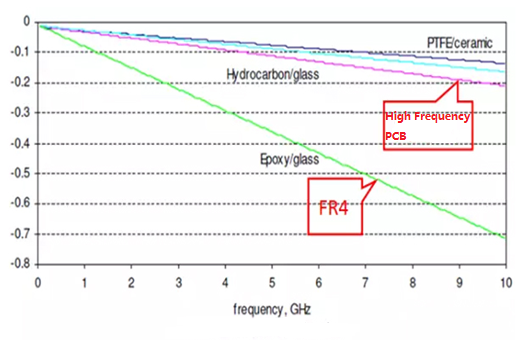
As clearly illustrated in the figure below, the signal loss characteristics vary significantly across different material grades. For instance, Ultra Low Loss materials exhibit a loss factor at 10GHz that is several times lower than that of standard materials. This superior performance is critical for ensuring signal integrity over long-distance transmissions.
High-Frequency vs. High-Speed: A Material Focus Divergence
- High-Frequency (RF/Microwave) Focus: Prioritizes Dk stability. Applications include power amplifiers and radar systems (e.g., 24/77GHz). For demanding frequencies, PTFE-based materials are often essential.
- High-Speed Digital Focus: Prioritizes low Df absolute values. Materials are tiered by Df: Standard Loss, Low Loss, Very Low Loss, etc., to match specific data rate requirements (e.g., 56G PAM4).
Beyond the Laminate: Copper and Manufacturing Synergy
- Copper Foil Roughness (Rz): The “skin effect” at high frequencies makes foil roughness a primary source of loss. Low-loss designs require Very Low Profile (VLP) copper.
- Precision Fabrication: Material potential is unlocked only through specialized processes.
- Tight Etch Tolerances: Coupled linewidths may require control to ±0.01mm.
- Plasma Treatment: PTFE materials need plasma treatment for reliable hole plating, unlike standard FR-4.
- Controlled Lamination: Strict protocols prevent delamination in multilayer boards.
To sum up, selecting high-frequency materials is a holistic decision integrating electrical requirements, material science, and manufacturing capability. The optimal laminate, when paired with precision fabrication, transforms from a simple substrate into the foundation of your product’s competitive edge.
What Are High Frequency PCB Materials and How They Influence Performance?
So, what exactly sets these materials apart? Standard FR-4 epoxy-glass laminates exhibit significant signal loss (dissipation factor) and less stable dielectric constant (Dk) at higher frequencies. This makes them unsuitable for demanding applications. High frequency PCB materials are engineered to overcome these limitations.
They primarily fall into several categories:
- PTFE-Based Composites: Materials like Rogers RO3000® series. PTFE (Teflon™) offers exceptionally low loss, making it ideal for extremely high-frequency applications like millimeter-wave radar. Its softness, however, requires specialized processing skill.
- Ceramic-Filled PTFE Composites: These materials, such as Rogers RO4000® series, blend PTFE with ceramic particles. This improves the Dk stability and mechanical properties for easier fabrication, offering a great balance of performance and manufacturability.
- Hydrocarbon-Based Ceramic Composites: Materials like Arlon’s 25N or Isola’s Tachyon® series. They provide excellent electrical properties and are more compatible with standard FR-4 multi-layer lamination processes, often reducing cost.
- Specialized Substrates: This includes aluminum backed PCB for excellent thermal management, and polyimide-based materials for high temperature environments.
The performance influence is profound. A low dissipation factor minimizes energy converted to heat, allowing signals to travel farther with less loss. A stable Dk ensures consistent impedance, which is the cornerstone of high frequency PCB design. Furthermore, these materials must withstand the high temperatures involved in assembly and operation. Ultimately, the theoretical advantages of these materials are only realized through a manufacturer’s ability to process them without compromising their inherent properties.
High Frequency PCB Design Guidelines: From Material Selection to Layout
Designing a successful high-frequency board requires a holistic approach. Your material selection and layout rules are deeply intertwined. Here are some essential high frequency pcb design guidelines to consider:
- Prioritize Impedance Control: This is non-negotiable. Your design must specify controlled impedance for critical traces. Work with your manufacturer early to determine the correct trace width and spacing for your chosen material’s Dk and board stack-up.
- Minimize Dielectric Loss: Select a material with a low dissipation factor (Df) for your target frequency. The higher the frequency, the lower the Df needs to be to avoid excessive signal attenuation.
- Manage Trace Geometry: Avoid sharp 90-degree bends; use curved or 45-degree traces instead to prevent impedance discontinuities and signal reflection.
- Plan Your Layer Stack-up Carefully: Use a symmetric stack-up to prevent warping. Shield sensitive signal layers with ground planes to contain electromagnetic fields and reduce crosstalk.
- Consider Thermal Expansion: Ensure the materials used in your PCB (copper, substrate) have compatible Coefficients of Thermal Expansion (CTE) to prevent delamination or broken vias during thermal cycling.
These guidelines highlight a critical point: material selection and design rules are a package deal. A manufacturer’s experience is what allows these design principles to be successfully implemented. They can advise on manufacturability, suggest stack-up adjustments, and ensure the final product matches your high frequency circuit design intent.
Selecting the Right PCB Material for High Frequency Applications
Choosing the optimal material is a balancing act between electrical performance, thermal requirements, mechanical needs, and cost. There is no single “best” material, only the best for your specific application. Ask these key questions:
- Above 10 GHz, low-loss PTFE-based materials are often necessary. Between 1-10 GHz, ceramic-filled PTFE or hydrocarbon ceramics may offer a better cost-to-performance ratio.
- High-power designs generate heat. You may need a material with high thermal conductivity, like an aluminum backed PCB or a specialized thermally conductive laminate.
- Will the board face extreme temperatures, humidity, or harsh chemicals? This may necessitate a material rated for high temperature or with low moisture absorption.
- If you need a complex multi-layer board, consider materials that are compatible with FR-4 in a hybrid construction to manage costs.
- For hybrid board material selection, high-frequency materials should be chosen according to customer requirements, with focus on dielectric constant and dissipation factor.
- For the FR-4 material, medium-high Tg grades should be selected, also focusing on Dk and Df – with priority given to S1000-2M and IT180A materials for hybrid constructions.
- For products with PIM requirements, special attention must be paid to the material’s PIM performance (typically -110 to -115 dBm).
A seasoned manufacturer has seen what works and what fails in real-world conditions. They can provide invaluable guidance, ensuring your material selection is not just theoretically sound but also practically optimal for manufacturing and long-term reliability.
| Supplier | Material Model | Tg (℃) | Td (℃) | Z-CTE (%) | Water Absorption (%) | Dk (@1GHz) | Df (@1GHz) |
| Shengyi | S1000H | ≥150 | ≥348 | 2.8 | 0.09 | 4.6 | 0.011 |
| S1000-2 | ≥170 | ≥345 | 2.8 | 0.1 | 4.8 | 0.013 | |
| S1000-2M | ≥170 | ≥340 | 2.4 | 0.08 | 4.6 | 0.018 | |
| Taiguang | EM825 | ≥150 | ≥340 | 3.2 | 0.1 | 4.3 | 0.016 |
| EM827 | ≥175 | ≥350 | 2.6 | 0.12 | 4.2 | 0.019 | |
| ITEQ | IT158 | ≥150 | ≥345 | 3.3 | 0.08 | 4.3 | 0.016 |
| IT180A | ≥170 | ≥345 | 2.7 | 0.12 | 4.4 | 0.015 |
Common High Frequency PCB Materials and Their Applications
Different materials shine in different applications. Here’s a brief look at some common high frequency PCB materials and where you’ll find them:
- Rogers RO4350B® (Ceramic-filled PTFE): A popular workhorse for power amplifiers, filters, and low-noise amplifiers in cellular infrastructure and automotive radar. It offers a good blend of electrical performance and ease of fabrication.
- Rogers RO3003® (PTFE-based): With an ultra-low loss tangent, it is ideal for demanding applications like satellite receivers, point-to-point radio links, and aerospace systems operating at Ka-band and above.
- Arlon 25N (Hydrocarbon Ceramic): Often used in GPS antennas, cellular base station antennas, and other applications where performance and cost-effectiveness are key. It laminates well with FR-4.
- Taconic TLY (PTFE-based): Known for its consistent Dk and low loss, it is frequently specified in critical phased-array radar systems and high-frequency test equipment.
- Aluminum Backed PCBs (Metal Core PCBs): While the metal core is typically aluminum, the circuit layer uses a high-frequency dielectric. These are essential for high-power LED lighting, RF power amplifiers, and any application where heat dissipation is a primary concern.
The choice of material directly impacts the final product’s high-frequency performance and field reliability. Selecting a material outside its optimal window can lead to premature failure or underperformance.
| Manufacturer | Model | Z-CTE (ppm/°C) | Water Absorption (%) | Dk (10 GHz) | Df (10 GHz) |
| Rogers | RO4350B | 32 | 0.05 | 3.48 | 0.0037 |
| RO4003C | 46 | 0.04 | 3.38 | 0.0027 | |
| RO4730G3 | 30.3 | 0.15 | 2.98 | 0.0029 | |
| RO3003 | 25 | 0.04 | 3 | 0.001 | |
| RO3006 | 24 | 0.02 | 6.15 | 0.002 | |
| RT/duroid 5880 | 173 | 0.02 | 2.33 | 0.0012 | |
| RT/duroid 5870 | 237 | 0.02 | 2.2 | 0.0009 | |
| Taconic | RF-10 | 25 | 0.08 | 10.2 | 0.0025 |
| RF-35 | 64 | 0.02 | 3.5 | 0.0018 | |
| TLX-8 | 140 | 0.02 | 2.55 | 0.0019 | |
| TLY-5 | 140 | 0.02 | 2.2 | 0.0019 | |
| Shengyi | S7136 | 30 | 0.06 | 3.42 | 0.003 |
| SCGA-500 GF220 | 217 | 0.01 | 2.2 | 0.0009 | |
| SCGA-500 GF255 | 145 | 0.01 | 2.55 | 0.0014 | |
| SCGA-500 GF265 | 95 | 0.01 | 3 | 0.002 | |
| SG5220 | 217 | 0.01 | 2.2 | 0.0009 |
Why Choose EBest Circuit (Best Technology) for Your High Frequency PCB Needs?
At BEST Technology, we understand that your success depends on getting every detail right. We are more than a board fabricator; we are your partner in high frequency PCB design and manufacturing. Our commitment to excellence is backed by:
- Advanced Manufacturing Infrastructure: We operate state-of-the-art equipment capable of handling the most delicate high-frequency laminates with precision.
- Rigorous Process Control: Our MES (Manufacturing Execution System) tracks every order in real-time, ensuring repeatability and traceability. We hold ISO 9001, IATF 16949, and AS9100D certifications, reflecting our unwavering commitment to quality.
- Expertise in High-Frequency Fabrication: Our engineering team possesses deep knowledge in precise lamination, impedance control (with tolerances as tight as ±5% or better), and low-loss processing techniques specific to high frequency PCB materials.
- High-Volume Capability Without Compromise: We are equipped for high volume PCB manufacturing, delivering consistent quality across large production runs.
We bridge the gap between material science and manufacturing excellence. We take the inherent advantages of your chosen high frequency materials and translate them into a high-performance, reliable finished product.
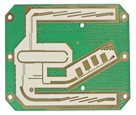
Case of High Frequency Materials PCB Fabrication by EBest Circuit (Best Technology)
In the realm of high-frequency applications, signal integrity is paramount. EBest Circuit (Best Technology) leverages advanced manufacturing techniques and a comprehensive material portfolio to deliver specialized PCB solutions for demanding wireless and high-speed digital products, ensuring superior performance and reliability.
Primary Applications:
- Wireless Communication Infrastructure: 5G/6G base stations, antenna arrays (e.g., AAUs), RF/microwave modules, satellite communication equipment.
- Automotive Electronics: Advanced Driver-Assistance Systems (ADAS), automotive radar (e.g., 77GHz), vehicle-to-everything (V2X) systems.
- Aerospace & Defense: Radar systems, avionics, navigation equipment, electronic warfare systems.
- High-Speed Data Communication: Network servers, routers, switches, optical transceivers.
- High-Performance Computing (HPC): AI/ML accelerator cards, supercomputers.
Key Technical Parameters & Process Capabilities for High-Frequency PCBs:
| Category | Standard Process Capability (Prototype/Production) | Advanced Process Capability (Limited to Prototype) |
|---|---|---|
| Core Materials | • PTFE-Based • Ceramic-Filled • Low-Loss/Speed Materials | |
| Layer Count | 1 – 50 Layers | Up to 100 Layers (≥50 layers require engineering review) |
| Board Thickness | 0.4mm – 6.0mm | 0.15mm – 10.0mm |
| Copper Thickness (Outer) | 0.5oz – 2oz | Up to 3oz |
| Copper Thickness (Inner) | 0.5oz – 1oz | Up to 2oz |
| Min. Line/Space (Outer, 1oz) | 3.5mil / 4mil | 3mil / 3mil |
| Min. Laser Drill Diameter | 0.10mm (Aspect Ratio ≤ 1:1) | 0.070mm (Aspect Ratio ≤ 1:1) |
| Min. Mechanical Drill Diameter | 0.15mm | 0.15mm |
| Impedance Control Tolerance | ±10% (for impedance ≥50Ω) | ±6% (for impedance ≥50Ω) |
In a nutshell, EBest Circuit (Best Technology) possesses end-to-end manufacturing capabilities for high-frequency PCBs, from material selection and precision patterning to lamination and final finishing. We focus on maintaining the stability of dielectric constant (Dk) and dissipation factor (Df), supported by stringent impedance control and advanced drilling technologies to provide reliable, high-performance circuit boards for cutting-edge applications. Our engineering team is available for consultation on specific requirements or special processes.
In conclusion, high frequency PCB materials are the critical starting point for any successful high-speed electronic device. Choosing the right substrate and partnering with a manufacturer who can faithfully build your design is the proven path to success. At BEST Technology, we provide the material guidance, manufacturing precision, and quality assurance you need to bring your most advanced products to market. Pls feel free to contact our experts at sales@bestpcbs.com for any high frequency materials PCB inquiries.
FAQs
Q1: What Tg values can your PCBs support? What are the benefits of high-Tg materials?
We commonly fabricate boards with Tg130, Tg150, and Tg170. We also have the capability to produce boards with high-Tg materials up to Tg260.
Generally, a Tg above 130°C is standard, while high-Tg is classified as above 170°C, and mid-Tg is above 150°C. An increased Tg value enhances the board’s properties, including:
- Heat resistance
- Moisture resistance
- Chemical resistance
- Overall stability
Higher Tg is particularly important for lead-free HASL processes, as it ensures the board can withstand higher temperatures.
Q2: What is the maximum board size you can produce?
Our standard maximum finished board size is 610mm x 610mm.
Q3: What is the maximum number of layers you can achieve in a PCB?
We can manufacture multilayer PCBs with up to 32 layers.
Q4: What is the minimum thickness you can achieve for different layer counts?
Our standard minimum thickness capabilities are as follows:
- Single/Double-sided boards: 0.15mm ±0.1mm
- 4-layer boards: 0.38mm ±0.1mm
- 6-layer boards: 0.5mm ±0.1mm
Q5: What is the smallest hole size you can drill?
We can drill micro-vias with a minimum finished diameter of 0.1mm.
Q6: Which PCB laminate brands do you commonly use?
We regularly work with several major, high-quality laminate brands, including:
- Shengyi (Shenyi)
- Kingboard (KB)
- ITEQ
- GDM
We can also source other brands based on your design requirements.